Top gate structure and preparation method thereof, thin film transistor, array substrate and display device

A thin-film transistor and top-gate technology, applied in transistors, semiconductor devices, electrical components, etc., can solve problems such as the decline of electrical performance of thin-film transistors, and achieve the effect of reducing process difficulty, reducing manufacturing process, and improving performance

Active Publication Date: 2016-08-10
BOE TECH GRP CO LTD
View PDF4 Cites 10 Cited by
  • Summary
  • Abstract
  • Description
  • Claims
  • Application Information

AI Technical Summary

Problems solved by technology

[0004] The purpose of the present invention is to overcome the problem of the decrease in the electrical performance of thin film transistors caused by the increase of the offset region, and

Method used


Image

  • Top gate structure and preparation method thereof, thin film transistor, array substrate and display device
  • Top gate structure and preparation method thereof, thin film transistor, array substrate and display device
  • Top gate structure and preparation method thereof, thin film transistor, array substrate and display device

Examples


Embodiment 1

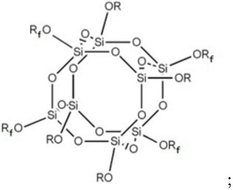
[0046] This embodiment provides a top gate structure, including a gate insulating layer and a gate layer above it, and the gate insulating layer is made of cage polysilsesquioxane;

[0047] The structure of the cage polysilsesquioxane is as follows:

[0048]

[0049] Among them, R represents the photosensitive group R f Represents the hydrophobic group-CF 3 、-CF 2 CF 3 or -CF 2 CF 2 CF 3 .

Embodiment 2

[0051] This embodiment provides a top gate structure, including a gate insulating layer and a gate layer above it, and the gate insulating layer is made of a linear silicone resin;

[0052] The structure of the linear silicone resin is as follows:

[0053]

[0054] Among them, R represents the photosensitive group R f Represents the hydrophobic group-CF 3 、-CF 2 CF 3 or -CF 2 CF 2 CF3 , n is 1, 2 or 3.

Embodiment 3

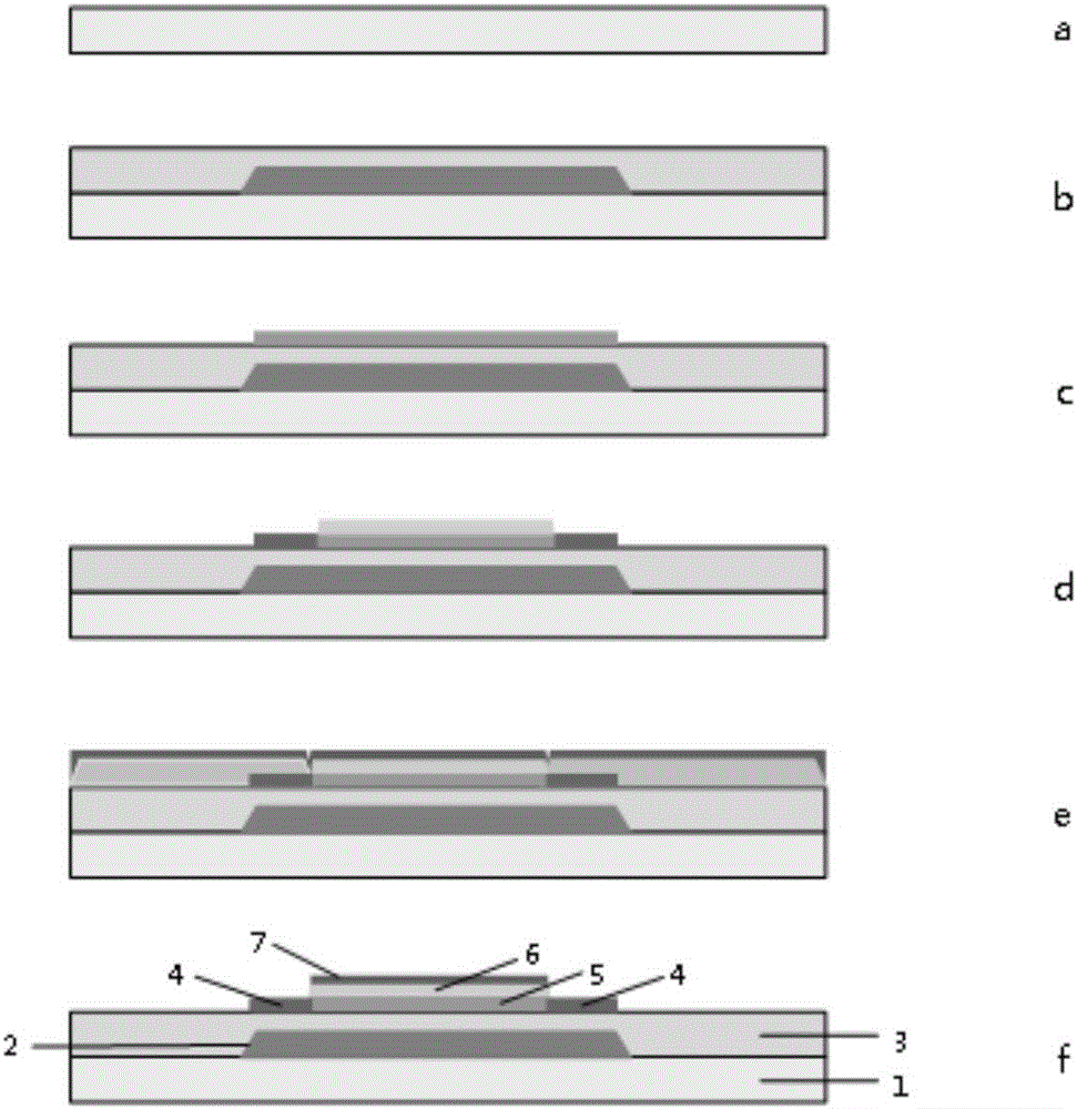
[0056] This embodiment provides a method for preparing a top-gate structure, which includes the following specific steps: apply a layer of photocurable organic silicon material by spin coating, dry after exposure and development to form a gate insulating layer; On the outside of the layer, apply a layer of thermosetting material by slit coating, place it in an oven for curing, and ensure that the gate insulating layer and the upper surface of the thermosetting material form a plane, and on this plane, use sputtering Spray coating a layer of metal used for preparing the gate layer; remove the cured heat-cured material and the metal above it by stripping.

[0057] The method described in embodiment 1 or 2 can be prepared by the method described in this embodiment.


PUM

PropertyMeasurementUnit
Thicknessaaaaaaaaaa
Thicknessaaaaaaaaaa
Thicknessaaaaaaaaaa

Abstract

The invention relates to a top gate structure and a preparation method thereof. The top gate structure comprises a gate insulation layer and a gate layer arranged on the gate insulation layer, wherein the gate insulation layer is made of a light-cured organosilicon material. The invention further relates to a thin film transistor comprising the top gate structure, an array substrate and a display device. Through the gate insulation layer made of the light-cured organosilicon material, and through the optimized preparation method, an offset region can be reduced, and the problem of reduction of the electrical performance of the thin film transistor due to enlargement of the offset region and the like is prevented; and the top gate structure has wide application prospect.

Description

technical field [0001] The invention relates to the field of display technology, in particular to a top gate structure and a preparation method thereof, as well as a thin film transistor containing the top gate structure, an array substrate and a display device. Background technique [0002] In the top-gate thin-film transistor technology, there is no overlap between the gate of the thin-film transistor and the S / D electrode, so the parasitic capacitance is very low. At the same time, due to the flexible layout, it can be used in large-size OLEDs with high resolution, high refresh rate, narrow frame, and low power consumption. There are more advantages in product application. [0003] However, the prior art provides that the CD offset in processes such as wet etching is large, so that the gate layer is relatively small, resulting in the occurrence of offset regions (such as figure 1 As shown), and the increase of the offset region will lead to a decrease in the electrical p...

Claims


Application Information

Patent Timeline
IPC IPC(8): H01L29/51H01L29/786
CPCH01L29/51H01L29/7869
Inventor 李伟宋泳锡张建业
Owner BOE TECH GRP CO LTD
Why Eureka
Try Eureka