Inverted green light quantum dot film electroluminescence device

A technology for electroluminescent devices and quantum dots to emit light, which is applied in the direction of electro-solid devices, electrical components, semiconductor devices, etc. question

Inactive Publication Date: 2016-08-10
SHANGHAI UNIV
View PDF5 Cites 10 Cited by
  • Summary
  • Abstract
  • Description
  • Claims
  • Application Information

AI Technical Summary

Problems solved by technology

[0003] However, holes in traditional quantum dot thin film electroluminescent devices (QLED) are not easy to inject, and hole injection materials with high HOMO (Highest Occupied Molecular Orbital, highest occupied molecular orbital) energy level are needed to help hole injection
Especially for green light quantum dot thin film electroluminescent devices, the HOMO energy level of green lig

Method used


Image

  • Inverted green light quantum dot film electroluminescence device
  • Inverted green light quantum dot film electroluminescence device
  • Inverted green light quantum dot film electroluminescence device

Examples


preparation example Construction

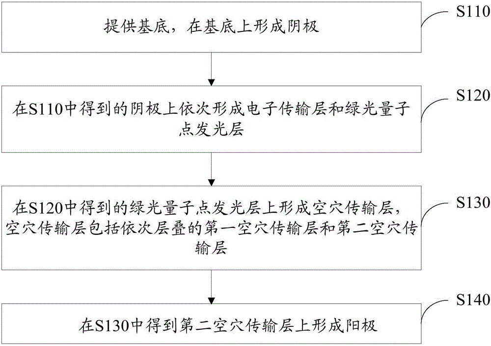
[0049] In addition, the present invention also provides a method for preparing the above-mentioned inverted green light quantum dot thin film electroluminescent device 10, such as image 3 As shown, the method includes the following steps S110-S140.

[0050] S110, providing a substrate, and forming a cathode on the substrate.

[0051] The material of the substrate can be glass, and the substrate can be ultrasonically treated with detergent, acetone, ethanol and isopropanol for 15 minutes each. Then vapor deposition, sputtering, sputtering or electrochemical vapor deposition on the substrate to form the cathode. The material of the cathode can be indium tin oxide (ITO), fluorine-doped tin oxide (FTO), aluminum-doped zinc oxide (AZO), indium-doped zinc oxide (IZO), etc., and the thickness of the cathode is 80nm-200nm.

[0052] Preferably, indium tin oxide (ITO) is sputtered onto the glass substrate by sputtering.

[0053] In this embodiment, after the cathode is formed on the...

Embodiment 1

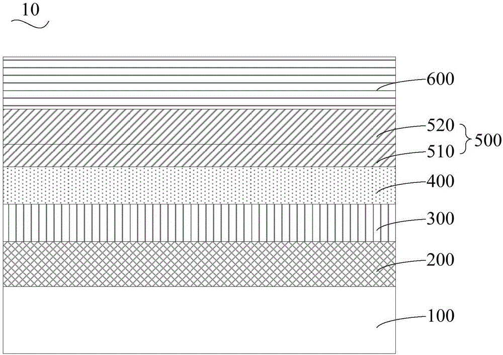
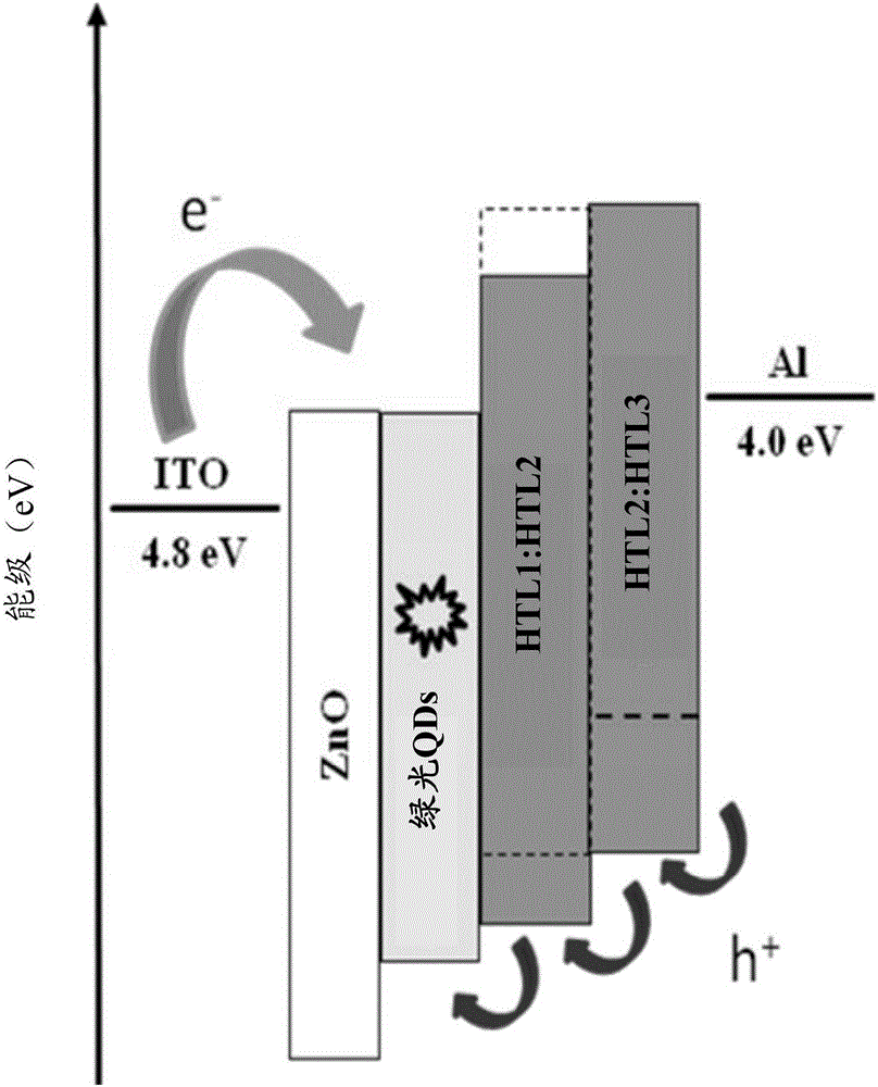
[0065] The structure of the inverted green light quantum dot thin film electroluminescent device is a substrate, a cathode, an electron transport layer, a green light quantum dot light-emitting layer, a hole transport layer and an anode, wherein the hole transport layer includes a laminated first hole transport layer and a second hole transport layer. hole transport layer. The first hole transport layer is in direct contact with the green light quantum dot light emitting layer. Wherein, the thickness of the first hole transport layer is 8 nm, and the material of the first hole transport layer is a mixture of the first hole transport material (HTL1) and the second hole transport material (HTL2), wherein HTL1 is 2- Hydroxy-3-methyl-2-cyclopenten-1-one (mCP), HTL2 is 8,8-bis(4-(9hydro-carbazol-9-yl)phenyl)-8hydro-indole [3,2,1-de]acridine (FPCC), the mass ratio of mCP to FPCC is 2:1. The thickness of the second hole transport layer is 25nm, and the second hole transport layer i...

Embodiment 2

[0071] The thickness of the first hole transport layer in the inverted green light quantum dot thin film electroluminescence device of the present embodiment is 5nm, and the material of the first hole transport layer is the mixture that HTL1 and HTL2 form, and wherein HTL1 is mCP, and HTL2 is FPCC, The mass ratio of mCP to FPCC is 4:3. The thickness of the second hole transport layer is 15nm, and the material of the second hole transport layer is a mixture of HTL2 and HTL3, wherein HTL2 is FPCC, and HTL3 is WO 3 , FPCC and WO 3 The mass ratio is 3:4. All the other are identical with embodiment 1.

[0072] The specific preparation method of the inverted green light quantum dot thin film electroluminescent device is the same as that of Example 1.

[0073] The HOMO energy level of the first hole transport layer was 6.1 eV, and the HOMO energy level of the second hole transport layer was 6.03 eV.

[0074] The brightness test was carried out on the prepared inverted green light...


PUM

PropertyMeasurementUnit
Thicknessaaaaaaaaaa
Thicknessaaaaaaaaaa
Thicknessaaaaaaaaaa

Abstract

The invention discloses an inverted green light quantum dot film electroluminescence device. The device comprises a substrate, a cathode, an electron transmission layer, a green light quantum dot luminescence layer, a hole transmission layer and an anode which are sequentially laminated, wherein the hole transmission layer comprises a first hole transmission layer and a second hole transmission layer which are laminated, and thickness of the first hole transmission layer is 5-15nm. According to the device, the HOMO energy level of the first transmission layer is greater than the HOMO energy level of the second transmission layer, so step type barrier is formed between the green light quantum dot luminescence layer and the anode, hole injection capability of the hole transmission layer is gradually improved, and hole injection requirements of the green light quantum dot film electroluminescence device can be satisfied.

Description

technical field [0001] The invention relates to the technical field of light-emitting devices, in particular to an electroluminescent device with an inverted green light quantum dot thin film. Background technique [0002] Quantum dots (QDs, quantum dots) are some extremely small semiconductor nanocrystals that cannot be seen by the naked eye, and the particle size is generally less than 10nm. When stimulated by light or electricity, quantum dots can emit colored light. The color of light is determined by the composition, material, size and shape of quantum dots. This feature enables quantum dots to change the color of light emitted by the light source. Because electrons, holes, and excitons are quantum-confined in the three-dimensional direction, the energy band structure of QDs changes from a bulk continuous structure to a discrete energy level structure with molecular characteristics. When the particle size of QDs is equal to or smaller than the Bohr radius of Wannier ex...

Claims


Application Information

Patent Timeline
IPC IPC(8): H01L51/50H01L51/54
CPCH10K50/11H10K2101/40H10K50/115H10K50/156H10K2102/321
Inventor 曹进周洁谢婧薇魏翔俞浩健
Owner SHANGHAI UNIV
Why Eureka
Try Eureka