Chip structure for effectively increasing PN junction area and manufacturing method thereof

A chip structure and PN junction technology, which is applied in semiconductor/solid-state device manufacturing, electrical components, electric solid-state devices, etc., can solve the problems of increasing chip cost and increasing the area of ​​PN junctions, etc., and achieve the effect of increasing the area

Inactive Publication Date: 2016-08-17
ZHEJIANG MINGDE MICROELECTRONICS CO LTD
View PDF7 Cites 8 Cited by
  • Summary
  • Abstract
  • Description
  • Claims
  • Application Information

AI Technical Summary

Problems solved by technology

If you want to increase the rated operating current of the chip, but you cannot increase the rated current density per unit area to make the operating junction temperature exceed the rated value, the existing method is to increase the size of the chip to achieve it, increasing the size of the chip, That is to say, the junction area of ​​the PN junction is increased. This existing practice brings about a substantial increase in chip cost.

Method used


Image

  • Chip structure for effectively increasing PN junction area and manufacturing method thereof
  • Chip structure for effectively increasing PN junction area and manufacturing method thereof
  • Chip structure for effectively increasing PN junction area and manufacturing method thereof

Examples


Embodiment 1

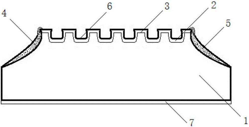
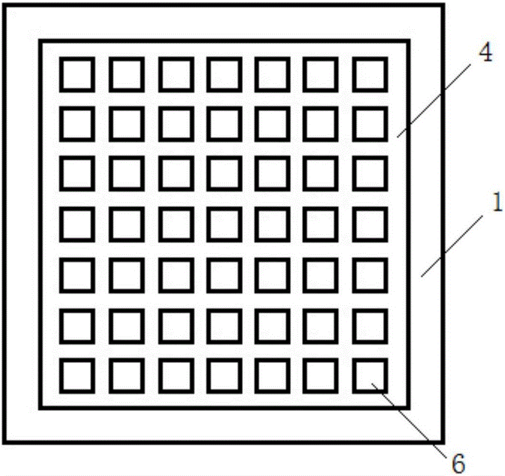
[0033] Embodiment 1: as figure 1 As shown, a chip structure that effectively increases the area of ​​the PN junction includes a chip body, the chip body includes a substrate layer 1, and one of the surfaces of the substrate layer 1 is provided with several equally spaced pits 6, and the cross-section of the pits 6 shaped like Figure 3 to Figure 6 As shown, it can be square, circular, hexagonal or annular, etc., and any pattern structure that can form the shape of the PN junction 3 in this embodiment is included; The heavily doped layer 2 with the opposite conductivity type forms a PN junction 3 at the intersection between the substrate layer 1 and the heavily doped layer 2, and the PN junction 3 is formed by a number of U-shaped curved surface junctions connected front and back, in which the U-shaped The middle part of the surface knot is a plane knot. There is a boss 4 in the middle of the side of the chip body with the pit 6, the PN junction is exposed on the side of the...

Embodiment 2

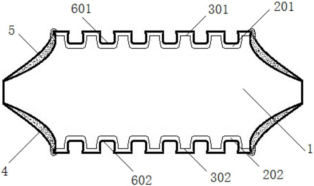
[0039] Embodiment 2: as figure 2 As shown, a chip structure that effectively increases the area of ​​the PN junction includes a chip body, the chip body includes a substrate layer 1, the upper surface of the substrate layer 1 is provided with a number of equally spaced pits 601, and the lower surface of the substrate layer 1 is also There are several equally spaced pits 602 symmetrically. The pits 601 and 602 have the same shape, and their cross-sectional shapes are as follows: Figure 3 to Figure 6 As shown, it can be a square, a circle, a hexagon, or a ring, etc., and any graphic structure that can form the shape of the PN junction in this embodiment is included. The upper surface of the chip body is doped to form a heavily doped layer 201 of the opposite conductivity type to the substrate layer 1, and the first PN junction 301 is formed at the intersection between the substrate layer 1 and the heavily doped layer 201; on the lower surface of the chip body doping to form a...

Embodiment 3

[0045] Embodiment 3: as Figure 7As shown, a chip structure that effectively increases the area of ​​the PN junction includes a chip body, the chip body includes a substrate layer 1, and one of the surfaces of the substrate layer 1 is doped to form a heavily doped layer 2 of a conductivity type opposite to that of the substrate layer 1, The intersection between the substrate layer 1 and the heavily doped layer 2 forms a PN junction 3, and the PN junction 3 is formed by connecting a number of U-shaped curved surface junctions front and back, wherein the middle part of the U-shaped curved surface junction is a planar junction, and the PN junction 3 is exposed on the surface where the heavily doped layer 2 is located, and the exposed part of the PN junction 3 is covered with a passivation layer 5. The passivation layer 5 is used to encapsulate the exposed PN junction 3 and isolate it from the outside world. The upper and lower surfaces of the chip body are uniform Covered with a ...


PUM


Abstract

The invention relates to a chip structure for effectively increasing the PN junction area and a manufacturing method thereof, and belongs to the technical field of semiconductors. The chip structure comprises a chip body, wherein the chip body comprises a substrate layer and a heavily doped layer which is reverse to the substrate layer in current conduction type and is formed by doping on one side or two sides of the substrate layer; a PN junction is formed on an intersection between the heavily-doped layer and the substrate layer; a naked part of the PN junction is covered with a passive layer; the upper surface and the lower surface of the chip body are covered with metal layers; the PN junction is formed by connecting a plurality of U-shaped curved surface junctions end to end; the middle parts of the U-shaped curved surface PN junctions are planar junctions. According to the chip structure, a plurality of U-shaped PN curved surface junctions are designed instead of an original planar PN junction, so that the area of the PN junction is increased effectively on the premise of not increasing the size of an original chip body, thereby fulfilling the aim of increasing the rated current of the chip on the basis of not increasing the manufacturing cost.

Description

technical field [0001] The invention relates to a chip structure and a manufacturing method thereof, in particular to a chip structure capable of effectively increasing the area of ​​a PN junction and a manufacturing method thereof, belonging to the technical field of semiconductors. Background technique [0002] Regardless of whether the semiconductor chip is working in the forward or reverse state, the current flowing through the PN junction will cause the chip to be heated and cause a temperature rise, and the temperature is the main factor affecting the thermal breakdown failure of the semiconductor chip. In order to prevent thermal breakdown failure of the chip, the operating junction temperature of the chip is generally limited to less than 120°C. [0003] The forward and reverse rated operating current of the chip is determined according to its rated operating junction temperature. Once the size of the chip is determined, it means that the junction area of ​​the PN ju...

Claims


Application Information

Patent Timeline
Patent Type & Authority Applications(China)
IPC IPC(8): H01L23/31H01L29/06H01L21/22
CPCH01L29/06H01L21/22H01L23/31
Inventor 谢晓东保爱林
Owner ZHEJIANG MINGDE MICROELECTRONICS CO LTD
Why Eureka
Try Eureka