Thin film package structure of display panel and fabrication method of thin film package structure

A thin-film packaging and display panel technology, used in semiconductor/solid-state device manufacturing, electrical components, electrical solid-state devices, etc., can solve problems such as easy cracking, water and oxygen infiltration, etc., to enhance conductivity, improve flexibility, and simple operation. Effect

Active Publication Date: 2016-08-17
GUANGDONG JUHUA PRINTING DISPLAY TECH CO LTD
View PDF4 Cites 9 Cited by
  • Summary
  • Abstract
  • Description
  • Claims
  • Application Information

AI Technical Summary

Problems solved by technology

[0004] The purpose of the present invention is to provide a thin-film packaging structure for display panels, aiming to solve the problem that the existing packaging technology of display panels is easy to produce cracks in flexible bending due to the ductility of the inorganic barrier layer, resulting in the penetration of water and oxygen

Method used


Image

  • Thin film package structure of display panel and fabrication method of thin film package structure
  • Thin film package structure of display panel and fabrication method of thin film package structure
  • Thin film package structure of display panel and fabrication method of thin film package structure

Examples


Embodiment Construction

[0021] In order to make the technical problems, technical solutions and beneficial effects to be solved by the present invention clearer, the present invention will be further described in detail below in conjunction with the embodiments. It should be understood that the specific embodiments described here are only used to explain the present invention, not to limit the present invention.

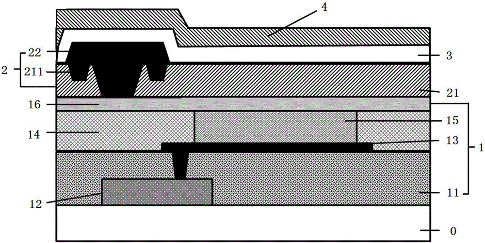
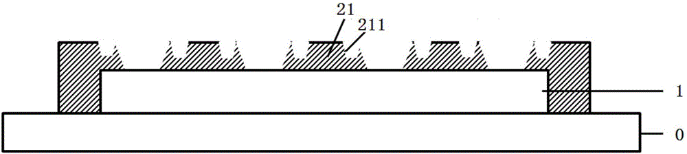
[0022] combine figure 1 , an embodiment of the present invention provides a thin film packaging structure for a display panel, including a metal / inorganic passivation layer 2, a buffer layer 3, and a second passivation layer 4 sequentially disposed on the top electrode 16 of a light emitting device 1, wherein, The metal / inorganic passivation layer 2 is composed of a metal sealing grid 22 and a plurality of independent inorganic passivation units 21 distributed in the metal sealing grid 22, and the inorganic passivation unit 21 completely covers the In the light emitting region 15 of the li...


PUM


Abstract

The invention provides a thin film package structure of a display panel and a fabrication method of the thin film package structure. The thin film package structure comprises a metal / inorganic passivation layer, a buffer layer and a second passivation layer which are sequentially arranged on a top electrode of a luminous device, wherein the metal / inorganic passivation layer comprises a metal sealing mesh and a plurality of independent inorganic passivation units, the plurality of independent inorganic passivation units are arranged in the metal sealing mesh, the inorganic passivation units completely cover a luminous region of the luminous device, and the metal sealing mesh is arranged on the surface of the top electrode on which the inorganic passivation units are not covered.

Description

technical field [0001] The invention belongs to the field of flat panel display technology, and in particular relates to a thin film packaging structure of a display panel and a preparation method thereof. Background technique [0002] In the present age of the information society, the importance of the display as a visual information transmission medium is further strengthened. In order to dominate in the future, displays are trending toward lighter, thinner, lower power consumption, lower cost, and better image quality. [0003] Organic light-emitting diode (OLED) has the advantages of self-luminescence, fast response, wide viewing angle, high brightness, and thinness. However, OLED devices are sensitive to water and oxygen, and the penetration of water and oxygen has a great impact on the life of the device, so strict packaging is required. At present, the cutting-edge packaging technology is thin-film packaging. In this method, an packaging film is formed by superimpos...

Claims


Application Information

Patent Timeline
Patent Type & Authority Applications(China)
IPC IPC(8): H01L51/52H01L51/56
CPCH10K50/844H10K71/00
Inventor 陈亚文
Owner GUANGDONG JUHUA PRINTING DISPLAY TECH CO LTD
Why Eureka
Try Eureka