

Method for manufacturing GaP rough surface of four-element chip
A rough surface, chip technology, applied in the field of optoelectronics, can solve the problems of GaP not easy to corrode, not easy to corrode, etc., to achieve the effect of improving quality, stable quality and simple operation
- Summary
- Abstract
- Description
- Claims
- Application Information
AI Technical Summary
Problems solved by technology
Method used
Image

Examples
Embodiment 1
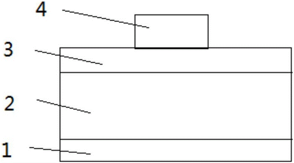
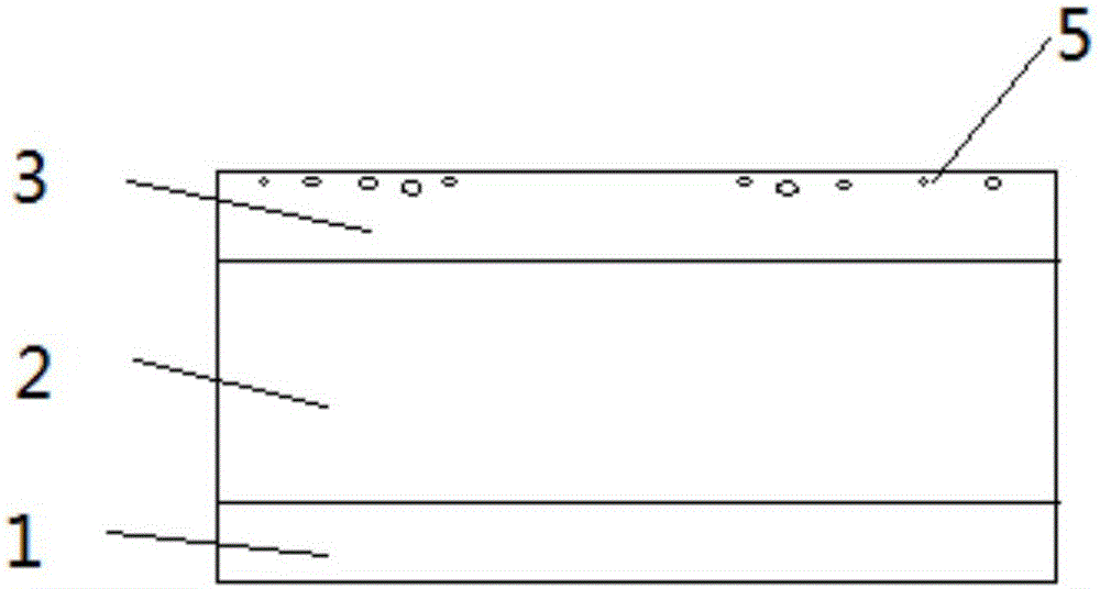
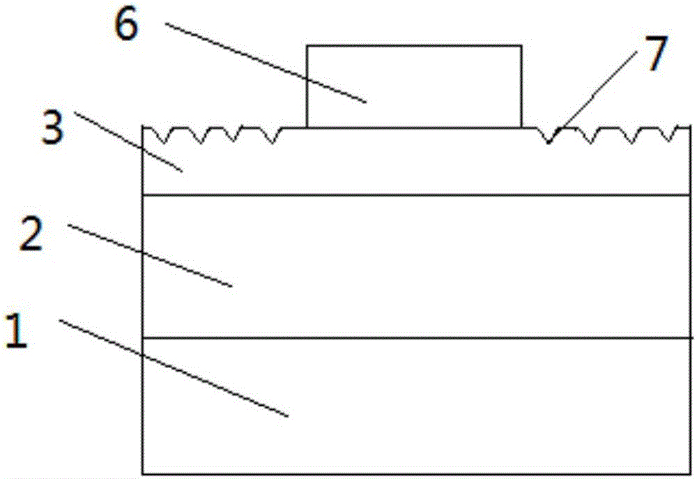
[0036] A method for preparing a GaP rough surface of a quaternary chip, comprising sequentially performing sandblasting roughening treatment and wet etching treatment on the GaP surface 3 to obtain a GaP rough light-emitting surface 7, the roughness range of the GaP rough light-emitting surface 7 : 0.5 μm<Ra<2 μm.
Embodiment 2
[0038] A method for preparing a GaP rough surface of a quaternary chip as described in Example 1, the difference is that the grit used in the sand blasting roughening treatment is: silicon carbide particles with a diameter of 12500 mesh to 15000 mesh.
Embodiment 3
[0040] The preparation method of the GaP rough surface of a kind of quaternary chip as described in embodiment 2, its difference is, described GaP surface is roughened by sandblasting 5-20 minutes, the included angle of sandblasting normal line and described GaP surface 70-90°, sandblasting speed 0.125-0.5cm / min, sandblasting grit density 0.5-2g / cm 2 .
PUM
| Property | Measurement | Unit |
|---|---|---|
| Roughness | aaaaa | aaaaa |
Abstract
Description
Claims
Application Information