Thermal activation sensitized phosphorescence organic electroluminescent light emitting device

A technique for sensitizing phosphorescence and electroluminescence

Active Publication Date: 2016-08-24
BEIJING VISIONOX TECH +1
View PDF2 Cites 28 Cited by
  • Summary
  • Abstract
  • Description
  • Claims
  • Application Information

AI Technical Summary

Problems solved by technology

This will lead to higher cost and at the same time cause the attenuation of device efficiency

Method used


Image

  • Thermal activation sensitized phosphorescence organic electroluminescent light emitting device
  • Thermal activation sensitized phosphorescence organic electroluminescent light emitting device
  • Thermal activation sensitized phosphorescence organic electroluminescent light emitting device

Examples


Embodiment 1

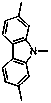
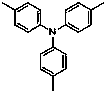
[0305] In this embodiment, light-emitting devices with different doping concentrations of thermally activated delayed fluorescent materials are prepared, and these devices have such as image 3 structure shown. The host material of the light-emitting layer (thermally activated delayed fluorescent material Host1 (1-9), thermally activated delayed fluorescent material Host2 (2-4), phosphorescent dye doped in the host material (Ir(ppy) 3 ). The thermally activated delayed fluorescent material Host2 (2-4) is an electron-transporting material, and the thermally activated delayed fluorescent material Host1 (1-9) is a hole-transporting material): ,

[0306] The device structure of this embodiment is as follows:

[0307] ITO (150nm) / NPB (40nm) / host material: (2%, 3%, 10%, 14%) phosphorescent dye (30nm) / Alq 3 (20nm) / LiF(0.5nm) / Al(150nm)

[0308] Wherein, the percentages in parentheses before phosphorescence represent different doping concentrations, and in this embodiment and...

Embodiment 2

[0329] In this embodiment, light-emitting devices with different doping concentrations of thermally activated delayed fluorescent materials are prepared, and these devices have such as image 3 structure shown. The host material of the light-emitting layer (thermally activated delayed fluorescent material Host 3 (1-4) , the adjustment host material (CBP), the phosphorescent dye Ir(piq) doped in the host material 3 . The thermally activated delayed fluorescent material Host 3 (1-10) is an electron-transporting material, and the adjusted host material CBP is a hole-transporting material, both of which have the same triplet energy level): The device structure of this embodiment is as follows:

[0330] ITO (150nm) / NPB (40nm) / host material: (2%, 3%, 10%, 14%) phosphorescent dye (30nm) / Alq 3 (20nm) / LiF(0.5nm) / Al(150nm)

[0331] Wherein, the percentages in parentheses before phosphorescence represent different doping concentrations, and in this embodiment and the following, ...

Embodiment 3

[0341] In order to test the influence of the host material of the present invention on the performance of the organic electroluminescent device, this example prepared an organic electroluminescent device in the same manner as in Example 1 above. The structure of the light emitting device is as follows:

[0342] ITO (150nm) / NPB (40 nm) / host material (the mass ratio of the two host materials is 1:1): 3% phosphorescent dye (Ir(ppy) 3 ) (30nm) / Bphen (20nm) / LiF (0.5nm) / Al (150nm).

[0343] The properties of the organic electroluminescent device are shown in Table 3 below:

[0344] table 3

[0345]


PUM


Abstract

The present invention discloses a thermal activation sensitized phosphorescence organic electroluminescent light emitting device which comprises a light emitting layer. The main body material of the light emitting layer is formed by two materials which are a hole-transporting material and an electron-transporting material. At least one material in the two materials is a thermal activation delay fluorescence material. The main body material is doped with a phosphorescent dye whose proportion is smaller than 15% by weight in the light emitting layer. The triplet energy level of the CT excitation state of the thermal activation delay fluorescence material is higher than the triplet energy level of an n-pi excitation state, and the difference is between 0 and 0.3 eV. Or, the triplet energy level of the CT excitation state of the thermal activation delay fluorescence material is higher than the triplet energy level of the n-pi excitation state, and the difference is larger than 1.0 eV, and the difference between the second triplet energy level of the n-pi excitation state and the first singlet energy level of the CT excitation state is between -0.1 eV and 0.1 eV.

Description

technical field [0001] The invention belongs to the field of organic electroluminescent devices, in particular to a heat-activated sensitized phosphorescent organic electroluminescent device. Background technique [0002] At present, in the prior art, the light-emitting layer of an organic electroluminescent device is generally composed of a host material doped with a dye. The traditional double-host light-emitting layer is composed of: a double-host doped dye (fluorescence or phosphorescence). The dual-host light-emitting layer The host material has no thermally delayed fluorescence effect, and the dye has no thermally delayed fluorescence property. [0003] Under electro-excitation conditions, organic electroluminescent devices will produce 25% singlet states and 75% triplet states. Traditional fluorescent materials can only utilize 25% of the singlet excitons due to spin prohibition, so the external quantum efficiency is only limited to within 5%. Almost all triplet exc...

Claims


Application Information

Patent Timeline
Patent Type & Authority Applications(China)
IPC IPC(8): H01L51/50H01L51/54
CPCC09K11/06H10K50/121H10K50/11H10K2101/40H10K2101/10H10K2101/90H10K2101/20H10K50/15C09K2211/1011C09K2211/1033C09K2211/1029H10K85/626H10K85/633H10K85/6572H10K50/00H10K85/636H10K85/657H10K50/12H10K85/624H10K2101/30C09K2211/1007C09K2211/1014C09K2211/1018
Inventor 段炼谢静刘嵩张东东赵菲
Owner BEIJING VISIONOX TECH
Why Eureka
Try Eureka