Self-aligning sintering clamp and method for semiconductor laser chip

A technology of lasers and semiconductors, which is applied in the direction of semiconductor lasers, lasers, laser components, etc., can solve the problems of inapplicability to batch sintering, difficulty in processing and assembling precision parts, and lower pressing pressure, so as to achieve convenient and reliable operation and inspection. The effect of reducing sintering voids and improving sintering yield

Active Publication Date: 2016-08-24
Shandong Huaguang Optoelectronics Co. Ltd.
View PDF4 Cites 8 Cited by
  • Summary
  • Abstract
  • Description
  • Claims
  • Application Information

AI Technical Summary

Problems solved by technology

The disadvantage of this method is that it is necessary to place heat sinks, chips and drop pressing pins under the microscope, which is inconvenient to operate and low in efficiency; and there are many parts in the whole device, it is difficult to process and assemble the precision parts required, and vacuum is required The equipment creates negative pressure to absorb heat sinks and chips, the manufacturing cost of the equipment is high, and it is not suitable for batch sintering
The disadvantage of this method is that the processing of the C-shaped bracket is relatively difficult; and after the heat sink and chip are placed on the alignment base and pushed into the positioning slot of the bracket, the chip on the heat sink cannot be observed due to the occlusion of the upper part of the bracket Whether there is any displacement during the placement process; in addition, during the thermal cycle of sintering, the spring used will undergo plastic deformation, resulting in a decrease in the pressing pressure, which may cause poor sintering of the chip

Method used


Image

  • Self-aligning sintering clamp and method for semiconductor laser chip
  • Self-aligning sintering clamp and method for semiconductor laser chip
  • Self-aligning sintering clamp and method for semiconductor laser chip

Examples


Embodiment 1

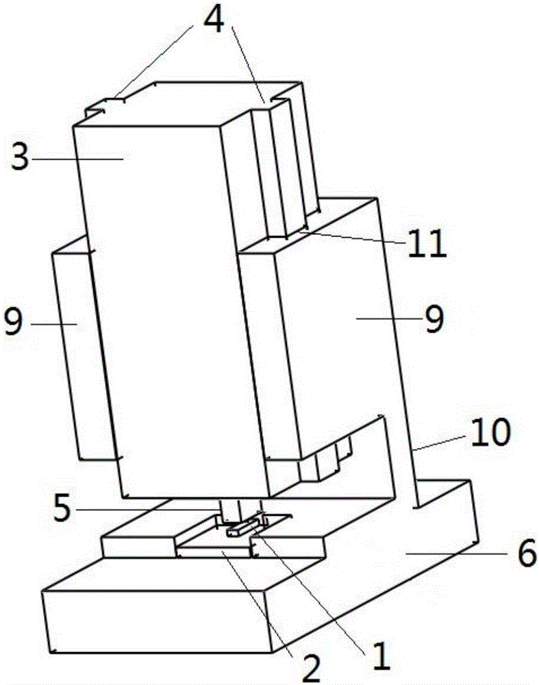
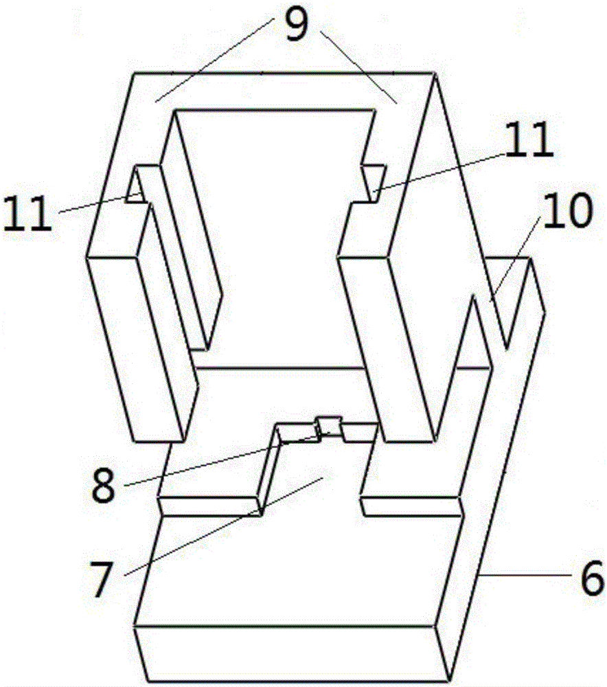
[0044] Self-aligned sintering fixtures for semiconductor laser chips, such as figure 1 As shown, it includes a base 6 , a guide rail bracket 10 and a pressing block 3 . The guide rail support is erected on the base, and there is a symmetrical cantilever 9 on the guide rail support, and a positioning guide rail 11 is arranged in the cantilever 9, and the positioning guide rail is a square groove. Such as image 3 shown. The base 6 has a positioning slot 7 that is compatible with the heat sink 2. The positioning slot 7 is a rectangular groove that is open on one side, so that the heat sink 2 can move in the positioning slot 7 and the side is attached to the inner wall of the slot. combine.

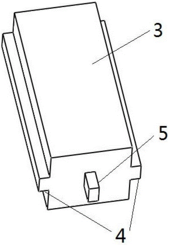
[0045] The structure of the briquetting block 3 is as figure 2 As shown, it includes a briquetting body 3, a briquetting positioning channel 4 and a briquetting post 5, and the size of the briquetting body 3 is adapted to the gap between the cantilevers 9 of the guide rail bracket; Roa...

Embodiment 2

[0051] Utilize the self-aligned sintering fixture of embodiment 1 to carry out the method for semiconductor laser chip sintering, the steps are as follows:

[0052] (1) place the semiconductor laser chip 1 on the solder on the heat sink 2 with an adsorption machine under a microscope;

[0053] (2) Insert the heat sink 2 loaded with the chip 1 into the positioning slot 7 of the base, and push it to the bottom;

[0054] (3) Observe from above with a microscope to confirm that the position of the laser chip 1 on the heat sink 2 has not shifted during operation;

[0055] (4) Place the pressing block positioning channels 4 on both sides of the pressing block in the positioning guide rail 11 of the cantilever on the guide rail bracket, insert the pressing block between the cantilevers and lower it, so that the lower end of the pressing column 5 is facing the laser chip 1 and pressing Tighten, complete the fixture clamping;

[0056] (5) Repeat the above steps (1) to (4), set up sev...


PUM


Abstract

The invention relates to a self-aligning sintering clamp and method for a semiconductor laser chip. The clamp comprises a pedestal, a guide rail support, and a press block. The pedestal is provided with a positioning card slot matched with a heat sink. Two sides of the press block are provided with symmetric positioning racks. The guide rail support is vertically disposed on the pedestal, and is provided with symmetric suspension arms. The interior of each suspension arm is provided with a positioning guide rail. The positioning racks of the press block can be sleeved by the positioning guide rails, and move up and down in the positioning guide rails. The bottom end of the press block is provided with a press column. When the press block moves downwards, the press column compresses a chip on the heat sink. The invention also provides the method for sintering the semiconductor laser chip through the above clamp. The clamp is simple in structure, is low in cost, can achieve the self-aligning, and is convenient for operation and observation. The method can achieve the quick batch sintering of the semiconductor laser chips and heat sinks, and remarkably improves the sintering yield of the clamp.

Description

technical field [0001] The invention relates to a self-aligning sintering jig for semiconductor laser chips and a chip sintering method using the jig, belonging to the technical field of semiconductor laser chip sintering. Background technique [0002] Due to the advantages of small size, light weight, high electro-optical conversion efficiency, long life and high reliability, semiconductor lasers have gradually replaced the use of gas and solid-state lasers in the fields of communication, medical treatment, display, industrial production and security. It is also gradually expanding. The waste heat generated by the chip when the semiconductor laser is working needs to be discharged in a timely and effective manner, otherwise it will cause the temperature of the laser chip to be too high, reduce the luminous efficiency of the device and induce the failure of the laser. The currently widely used technical solution is to sinter the semiconductor laser chip onto a heat sink wit...

Claims


Application Information

Patent Timeline
Patent Type & Authority Applications(China)
IPC IPC(8): H01S5/022
CPCH01S5/0237H01S5/02375
Inventor 杨扬徐现刚夏伟李沛旭
Owner Shandong Huaguang Optoelectronics Co. Ltd.
Why Eureka
Try Eureka