Supercharge Your Innovation With Domain-Expert AI Agents!

Low-junction-temperature photovoltaic junction box and chip assembly therefor

A junction box and junction temperature technology, applied in the field of low junction temperature photovoltaic junction boxes, can solve the problems of easy failure, high junction temperature of diodes, short life of photovoltaic modules in junction boxes, etc. Good cooling effect

Inactive Publication Date: 2016-08-24
黄子健
View PDF7 Cites 6 Cited by
  • Summary
  • Abstract
  • Description
  • Claims
  • Application Information

AI Technical Summary

Problems solved by technology

The limitation of the existing technology is that the junction temperature of the diode is too high, and it is difficult to further reduce it, which leads to the junction box becoming the shortest life of the photovoltaic module or the most prone to failure.

Method used


Image

  • Low-junction-temperature photovoltaic junction box and chip assembly therefor
  • Low-junction-temperature photovoltaic junction box and chip assembly therefor
  • Low-junction-temperature photovoltaic junction box and chip assembly therefor

Examples


Embodiment 1

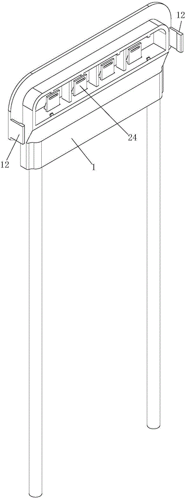
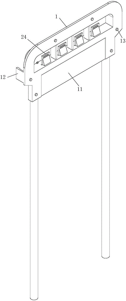
[0031] Reference attached figure 1 to attach Figure 4 , a low-junction temperature photovoltaic junction box, which includes a chip module 2, and a shell 1 wrapped outside the chip module 2.

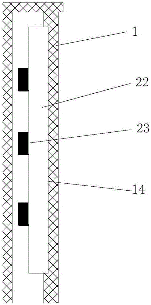
[0032] The chip module 2 includes a chip assembly, the chip assembly has a circuit surface with a circuit, and a heat dissipation surface opposite to the circuit surface, and the heat dissipation surface is in direct contact with the above-mentioned housing 1 .

[0033] The above-mentioned circuit face faces the back plate of the photovoltaic module connected with the casing. The photovoltaic module backplane can be a polymer backplane or a glass backplane.

[0034] There are many ways to connect the shell 1 and the chip assembly, such as attached image 3 In the present embodiment shown, a connection structure between the housing 1 and the chip assembly is provided: the inner side of the housing 1 has a groove 14, and the circuit surface of the chip assembly faces the groove 14 and ...

Embodiment 2

[0045] Reference attached Figure 5 The only difference between the low junction temperature photovoltaic junction box in this embodiment and the first embodiment is that in this embodiment, the housing 1 is integrally injection-molded on the chip module 2 and covers the chip module 2 .

[0046] In order to protect the circuit surface of the chip assembly from damage during the injection molding process of the housing 1 , the chip module 2 in this embodiment further includes a cover plate 21 connected with the chip assembly and covering the circuit surface of the chip assembly.

[0047] as attached Figure 5 As shown, the cover plate 21 covers the circuit surface of the chip assembly. One end of the terminal post 24 protrudes from the cover plate 21 . Reliability can be improved by dispensing epoxy glue between the cover plate 21 and the chip component (preferably at the diode). Due to the modular design of the chip, the chip module 2 can be directly embedded into the plast...


PUM


Abstract

The invention discloses a low-junction-temperature photovoltaic junction box and a chip assembly therefor. The junction box comprises a chip module and a housing covering the chip module. The chip module comprises a chip assembly, and the chip assembly is provided with a circuit surface with a circuit, and a heat dissipation surface opposite to the circuit surface. The heat dissipation surface directly contacts with the housing. The chip assembly for the junction box comprises an aluminum substrate, a plurality of diodes, and a plurality of binding posts, wherein the diodes and the binding posts are connected to the aluminum substrate. One surface, connected with the diodes and the binding posts, of the aluminum substrate is the circuit surface, and the other surface, opposite to the circuit surface, of the aluminum substrate is the heat dissipation surface. A conventional junction box is formed by the jointing of a box body and a heat dissipation copper piece. However, the housing of the junction box directly contacts with the heat dissipation surface of the chip assembly, thereby forming a body, and enabling the heat dissipation capability of the body to be stronger. The junction box removes an air (hollow junction box) or silica gel (gluing junction box) heat conducting layer, reduces the thermal resistance, and enables the heat dissipation capability to be stronger than the conventional junction box by several times.

Description

technical field [0001] The invention relates to a low junction temperature photovoltaic junction box and a chip component used for the low junction temperature photovoltaic junction box. Background technique [0002] The photovoltaic junction box is a connector between the solar cell array formed by solar cell components and the solar charging control device. Next, it acts as a shunt to ensure that the output of good cells will not be blocked due to poor cells (barrel effect). A photovoltaic junction box generally consists of a box body, cables and connectors, of which the box body is the main part, including the box body, internal metal copper sheets, diodes, box covers, etc., where the box body and the box cover are connected to form the junction box. shell. Existing photovoltaic junction boxes are mainly divided into junction boxes with glue filling and hollow structures. Wherein, the hollow junction box plays the effect of sealing the box cover and the box body throug...

Claims


Application Information

Patent Timeline
Patent Type & Authority Applications(China)
IPC IPC(8): H02S40/34
CPCH02S40/345H02S40/34Y02E10/50
Inventor 黄子健张菊
Owner 黄子健
Features
  • R&D
  • Intellectual Property
  • Life Sciences
  • Materials
  • Tech Scout
  • Unparalleled Data Quality
  • Higher Quality Content
  • 60% Fewer Hallucinations
Learn More