

Preparation method of GaN-based light emitting diode
A light-emitting diode, N-type technology, applied in the direction of electrical components, circuits, semiconductor devices, etc., can solve the problems of low luminous efficiency of GaN-based light-emitting diodes, achieve the effects of reducing dislocation defects, improving luminous efficiency, and improving crystal quality
- Summary
- Abstract
- Description
- Claims
- Application Information
AI Technical Summary
Problems solved by technology
Method used
Image


Examples
preparation example Construction
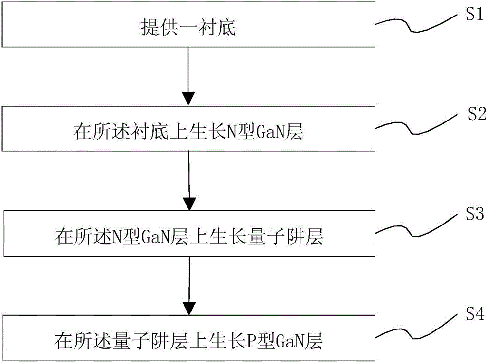
[0033] The core idea of the present invention is that the present invention provides a method for preparing a GaN-based light-emitting diode, such as figure 1 Shown: Include the following steps:
[0034] Step S1, providing a substrate;
[0035] Step S2, growing an N-type GaN layer on the substrate;
[0036] Step S3, growing a quantum well layer on the N-type GaN layer;
[0037] Step S4, growing a P-type GaN layer on the quantum well layer;
[0038] Wherein, the N-type GaN layer and / or the P-type GaN layer are grown by variable temperature, and the temperature in the variable temperature growth is a periodically fluctuating temperature.
[0039] The present invention grows the N-type GaN layer or / and the P-type GaN layer in a temperature-variable manner. Different growth temperatures can change the carbon content of the N-type GaN layer or / and P-type GaN layer. At the same time, different growth temperatures can change the N-type GaN layer. The lateral growth rate and ver...
Embodiment 1
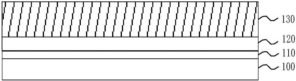
[0042] Such as figure 1 As shown, first, step S1 is performed, such as figure 2 As shown, a substrate 100 is provided. The material of the substrate 100 may be a sapphire substrate, a GaN substrate, a silicon substrate or a silicon carbide substrate.
[0043] Then, if figure 1 As shown, proceed to step S2, such as image 3 As shown, an N-type GaN layer 130 is grown on the substrate 100 . In actual production, a sequentially stacked buffer layer 110 and an undoped GaN layer 120 are formed between the substrate 100 and the N-type GaN layer 130 . The material of the buffer layer 110 is GaN, AlN or AlGaN, the growth temperature of the buffer layer 110 is 450°C-650°C, and the growth thickness is 15nm-50nm; the growth temperature of the undoped GaN layer 120 is 900°C ~1200°C.
[0044] The N-type GaN layer 130 is grown by variable temperature, and the temperature in the variable temperature growth is a periodically fluctuating temperature (wherein, the periodically fluctuating...
Embodiment 2
[0053] see Figure 7-Figure 9 , among which, in Figure 7-Figure 8 , the reference numerals indicate the same Figure 2-Figure 6 The same expression and the same structure in the preparation method of the first embodiment, the difference between the preparation method of the second embodiment and the preparation method of the first embodiment are:
[0054] Such as Figure 7 As shown, in step S2 of the preparation method, an N-type GaN layer 131 is grown on the substrate 100 at a fixed temperature. The growth temperature of the N-type GaN layer 131 is 700°C-1200°C, the growth thickness is 1.5um-4.5um, and the Si doping concentration of the N-type GaN layer 131 is 1e18cm -3 ~3e19cm -3 .
[0055] Such as Figure 8 As shown, in step S4 of the preparation method, a P-type GaN layer 181 is grown on the quantum well layer 140, and the P-type GaN layer 181 is grown by variable temperature, and the temperature in the variable temperature growth fluctuates periodically temperatur...
PUM
 Abstract
Description
Claims
Application Information