

Glitch-type PUF circuit employing delay tree structure
A burr-type, tree-structured technology, applied in logic circuits, electrical components, pulse processing, etc., can solve problems that affect the practical progress of PUF circuits
- Summary
- Abstract
- Description
- Claims
- Application Information
AI Technical Summary
Problems solved by technology
Method used
Image

Examples
Embodiment 1
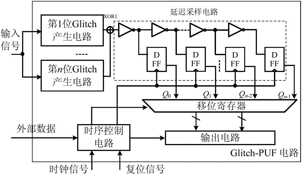
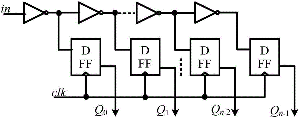
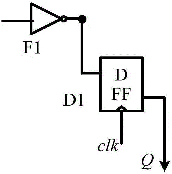
[0017] Embodiment one: if Figure 1-Figure 3 As shown, a glitch-type PUF circuit using a delay tree structure includes a timing control circuit, a shift register, a Glitch generation circuit with the same n-bit structure, a delay sampling circuit, an output circuit, and an n-input XOR gate XOR1, where n is an integer And 1≤n≤128; the delay sampling circuit includes a delay sampling unit with the same n-bit structure, the delay sampling unit includes a first inverter F1 and a D flip-flop D1, and the D flip-flop D1 has a clock terminal, an input terminal and an output terminal, The input end of the first inverter F1 is the input end of the delay sampling unit, the output end of the first inverter F1 is connected to the input end of the D flip-flop D1, and the output end of the D flip-flop D1 is the output end of the delay sampling unit , the clock terminal of the D flip-flop D1 is the clock terminal of the delay sampling unit, the clock terminal of the n-bit delay sampling unit ...
Embodiment 2
[0020] Embodiment two: if Figure 1-Figure 3 As shown, a glitch-type PUF circuit using a delay tree structure includes a timing control circuit, a shift register, a Glitch generation circuit with the same n-bit structure, a delay sampling circuit, an output circuit, and an n-input XOR gate XOR1, where n is an integer And 1≤n≤128; the delay sampling circuit includes a delay sampling unit with the same n-bit structure, the delay sampling unit includes a first inverter F1 and a D flip-flop D1, and the D flip-flop D1 has a clock terminal, an input terminal and an output terminal, The input end of the first inverter F1 is the input end of the delay sampling unit, the output end of the first inverter F1 is connected to the input end of the D flip-flop D1, and the output end of the D flip-flop D1 is the output end of the delay sampling unit , the clock terminal of the D flip-flop D1 is the clock terminal of the delay sampling unit, the clock terminal of the n-bit delay sampling unit ...
PUM
 Abstract
Description
Claims
Application Information