Printed circuit board and fully-additive manufacturing method therefor

A printed circuit board and manufacturing method technology, applied in the electronic field, can solve the problems of high cost and low production efficiency of printed circuit boards, and achieve the effects of high reliability, high production efficiency and good conductivity

Active Publication Date: 2016-09-07
UNIV OF ELECTRONICS SCI & TECH OF CHINA +1
View PDF6 Cites 9 Cited by
  • Summary
  • Abstract
  • Description
  • Claims
  • Application Information

AI Technical Summary

Problems solved by technology

[0007] The purpose of the present invention is to provide a printed circuit board and its full additive manufacturing method which solves the above problems. High cost and low production efficiency

Method used


Image

  • Printed circuit board and fully-additive manufacturing method therefor
  • Printed circuit board and fully-additive manufacturing method therefor
  • Printed circuit board and fully-additive manufacturing method therefor

Examples


Embodiment

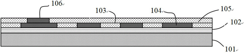
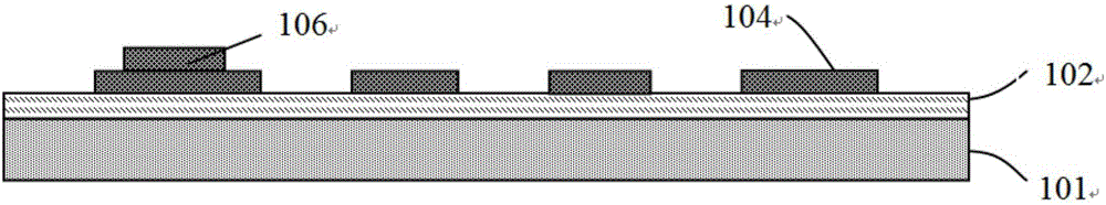
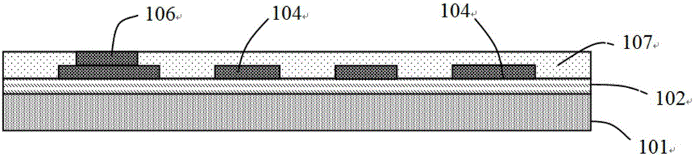
[0041] Embodiment: a kind of printed circuit board, see Figure 6 , the printed circuit board is mainly composed of a plurality of laminated first structures and second structures, the first structure and the second structure are distributed at intervals, and the first structure and the second structure are formed by hot pressing, and the The first structure is mainly composed of a circuit carrier. The circuit carrier is embedded with a conductive bump 106 and a circuit layer 104. The conductive bump 106 is electroplated on the circuit layer 104. The second structure is mainly composed of an insulating dielectric plate. The insulating medium plate is embedded with a conductive block 202, and the circuit layers on the two adjacent first structures are connected through the conductive block. The circuit carrier is a resin plate 107; the insulating medium plate is a prepreg 201, and the prepreg 201 As an interlayer bonding structure, the interconnection reliability of the interla...


PUM


Abstract

The invention discloses a printed circuit board. The printed circuit board mainly comprises multiple first structures and second structures which are overlapped in a lamination manner, wherein the first structures and the second structures are arranged at intervals; the first structures and the second structures are formed in a hot-pressing manner; the first structures mainly consist of circuit carriers; conductive convex blocks and circuit layers are embedded in the circuit carriers; the conductive convex blocks are electroplated on the circuit layers; the second structures mainly consist of insulating dielectric plates; conductive blocks are embedded in the insulating dielectric plates; and the circuit layers on the adjacent two first structures are connected through the conductive blocks. Compared with the prior art, the printed circuit board provide by the invention enables fine circuits to satisfy special impendence characteristic requirement; meanwhile, the prepared circuit is high in conductivity and low in cost; the first structures and the second structures are overlapped in a crossed manner in sequence, so that the printed circuit at any layer can be formed by one-time lamination; and therefore, the printed circuit board is high in production efficiency and capable of reducing the production time and the production cost.

Description

technical field [0001] The invention relates to the electronic field, in particular to a printed circuit board and a full-additive manufacturing method thereof. Background technique [0002] With the development of society and science and technology, electronic products are increasingly miniaturized. This development trend has also led to the development of printed circuit boards for connecting different devices and substrates for semiconductor chip packaging under the premise of ensuring good electrical and thermal properties. Develop in the direction of light, thin, short and small. In order to meet the above requirements, finer lines with smaller dimensions and thinner insulating layers are technical conditions that must be met. According to the classification of circuit formation methods, there are mainly three types of methods for circuit production, which are subtractive method, semi-additive method and full additive method. [0003] ① subtraction method. That is, o...

Claims


Application Information

Patent Timeline
Patent Type & Authority Applications(China)
IPC IPC(8): H05K1/11H05K3/20H05K3/46
CPCH05K1/119H05K3/205H05K3/4611H05K2201/0367
Inventor 何为胡志强陈苑明艾克华王守绪叶金洪何雪梅
Owner UNIV OF ELECTRONICS SCI & TECH OF CHINA
Why Eureka
Try Eureka