Thin film transistor, array substrate, display panel and display device

A technology of thin film transistors and array substrates, applied in the display field, can solve problems such as easy disconnection, and achieve the effects of reducing the occupied area, increasing the aperture ratio, and increasing the aspect ratio

Inactive Publication Date: 2016-09-21
BOE TECH GRP CO LTD +1
View PDF3 Cites 7 Cited by
  • Summary
  • Abstract
  • Description
  • Claims
  • Application Information

AI Technical Summary

Problems solved by technology

[0006] In view of this, an embodiment of the present invention provides a thin film transistor, an array substrate, a display panel, and a display device, which are used to increase the width-to-length ratio of the channel of the thin film transistor and avoid The problem that the source electrode is easy to break during the etching process

Method used


Image

  • Thin film transistor, array substrate, display panel and display device
  • Thin film transistor, array substrate, display panel and display device
  • Thin film transistor, array substrate, display panel and display device

Examples


example 1

[0038] Example 1: The above thin film transistor provided by the embodiment of the present invention is applied to a bottom gate thin film transistor.

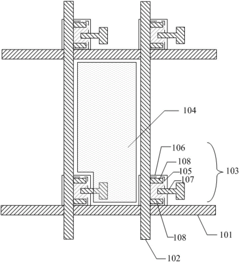
[0039] In specific implementation, in the above-mentioned thin film transistor provided by the embodiment of the present invention, such as Figure 4 as shown, Figure 4 for image 3 In the cross-sectional view along the AA direction, the active layer 2 is located above the gate electrode 1 ; the source electrode 3 and the drain electrode 4 are located above the active layer 2 .

[0040] Preferably, in the above-mentioned thin film transistor provided by the embodiment of the present invention, such as image 3As shown, the orthographic projection of the channel 5 on the gate electrode 1 can be set in the area where the gate electrode 1 is located, that is, the area of ​​the hollowed out part of the gate electrode 1 is smaller than or equal to the area of ​​the source electrode 3, so that the gate electrode 1 can block the c...

example 2

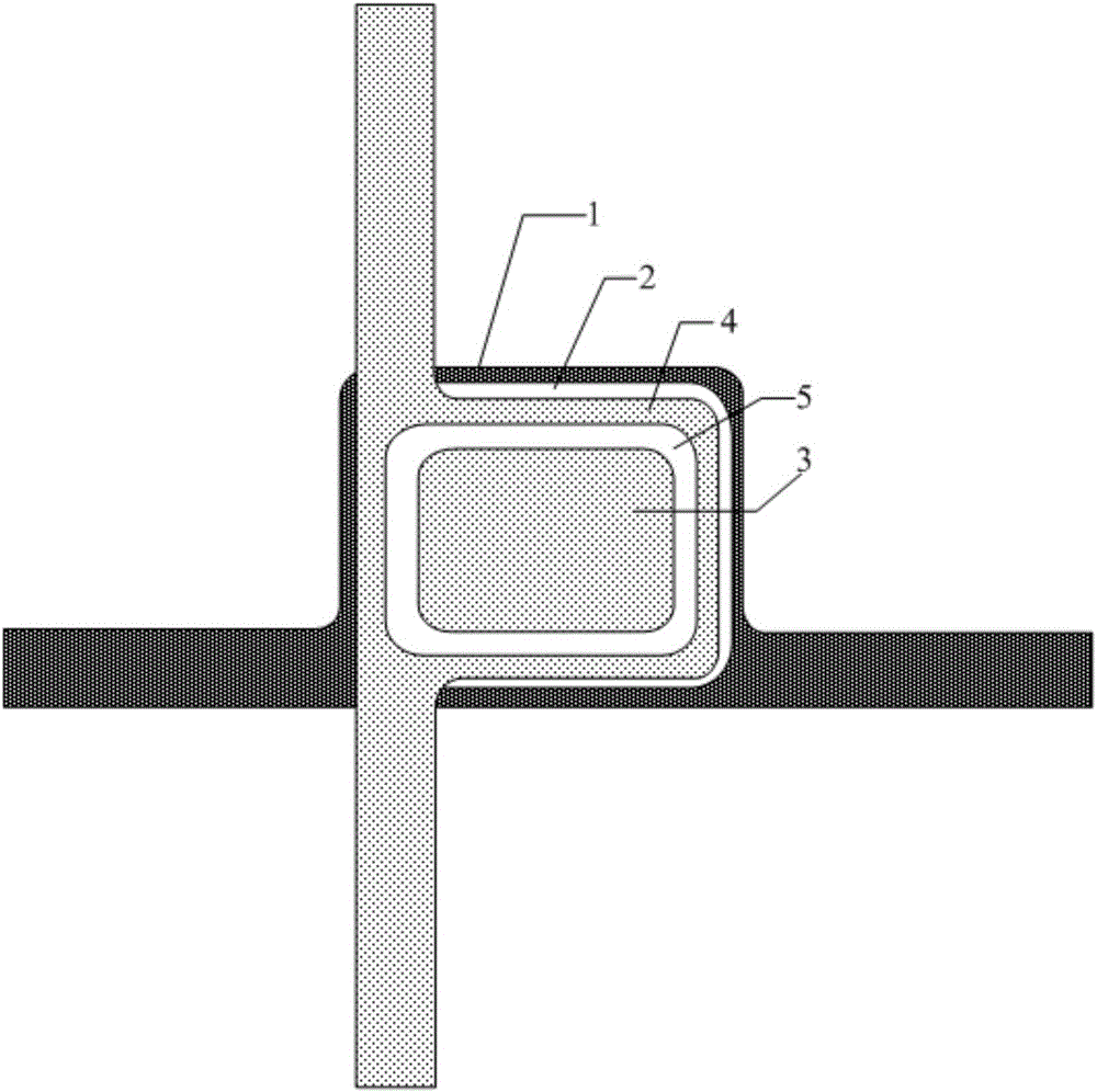
[0042] Example 2: The above-mentioned thin film transistor provided by the embodiment of the present invention is applied to a top-gate thin film transistor.

[0043] In specific implementation, in the above-mentioned thin film transistor provided by the embodiment of the present invention, such as Figure 5 As shown, the active layer 2 is located above the source electrode 3 and the drain electrode 4 ; the gate electrode 1 is located above the active layer 2 .

[0044] It should be noted that the specific implementation of Example 2 of the present invention is similar to the implementation of Example 1 of the present invention, and repeated descriptions will not be repeated.

[0045] Based on the same inventive concept, an embodiment of the present invention further provides an array substrate, including: the above-mentioned thin film transistor provided by the embodiment of the present invention. For the implementation of the array substrate, reference may be made to the ab...


PUM


Abstract

The invention discloses a thin film transistor, an array substrate, a display panel and a display device. The thin film transistor includes a mutually insulated gate electrode and an active layer, and a source electrode and a drain electrode respectively electrically connected to the active layer; The electrode surrounds the source electrode, and a closed channel is formed between the drain electrode and the source electrode. In this way, the width-to-length ratio of the channel can be increased, so that when the width-to-length ratio of the channel is constant, the occupied area of ​​the thin film transistor can be correspondingly reduced. , increase the aperture ratio of the display panel, and then can reduce the power consumption of the display panel correspondingly when the display panel displays the same brightness; and, since the source electrode is at the step formed by the gate electrode, the gate insulating layer and the active layer The shape of the electrode is not a thin line, therefore, the source electrode will not be broken or partially broken when the pattern of the source electrode is formed by etching, so as to avoid affecting the normal display of the display panel.

Description

technical field [0001] The invention relates to the field of display technology, in particular to a thin film transistor, an array substrate, a display panel and a display device. Background technique [0002] With the continuous development of display technologies, flat display panels such as organic electroluminescent display panels (Organic Electroluminescent Display, OLED) and liquid crystal display panels (Liquid Crystal Display, LCD) are developing rapidly. [0003] Taking a liquid crystal display panel as an example, it includes an array substrate, an opposite substrate, and a liquid crystal layer between the two substrates. Array substrates, such as figure 1 As shown, it includes: a base substrate, and gate lines 101, data lines 102, thin film transistors 103 and pixel electrodes 104 located on the base substrate; wherein, the thin film transistor 103 generally includes a gate electrode 105, an active layer 106, a source electrode 107 and a drain electrode 108 , wh...

Claims


Application Information

Patent Timeline
Patent Type & Authority Applications(China)
IPC IPC(8): H01L29/10H01L29/417H01L29/786H01L27/12
CPCH01L29/78696H01L27/1222H01L27/124H01L29/1033H01L29/41733H01L29/41758
Inventor 周厚峰黄中浩高坤坤毕鑫赵永亮
Owner BOE TECH GRP CO LTD
Why Eureka
Try Eureka