Eureka AIR delivers breakthrough ideas for toughest innovation challenges, trusted by R&D personnel around the world.

UV light emitting diode with compound electronic barrier layer structure

An electron blocking layer, light-emitting diode technology, applied in circuits, electrical components, semiconductor devices, etc., can solve the problems of low conductivity and low Mg activation efficiency, improve injection efficiency, prevent electrons from overflowing the active area, and improve luminescence. The effect of power

Active Publication Date: 2016-09-28
SOUTHEAST UNIV
View PDF8 Cites 18 Cited by
  • Summary
  • Abstract
  • Description
  • Claims
  • Application Information

AI Technical Summary

Problems solved by technology

[0004] The problem of the doping efficiency of p-type AlGaN materials is more prominent. The activation energy of Mg acceptors in p-type GaN at room temperature is 160-200meV, and the activation energy of Mg in AlGaN materials can reach up to 510-600meV, so the activation efficiency of Mg Very low, resulting in a much lower hole concentration in p-type AlGaN than in p-type GaN, and lower conductivity

Method used


Image

  • UV light emitting diode with compound electronic barrier layer structure
  • UV light emitting diode with compound electronic barrier layer structure
  • UV light emitting diode with compound electronic barrier layer structure

Examples


Embodiment

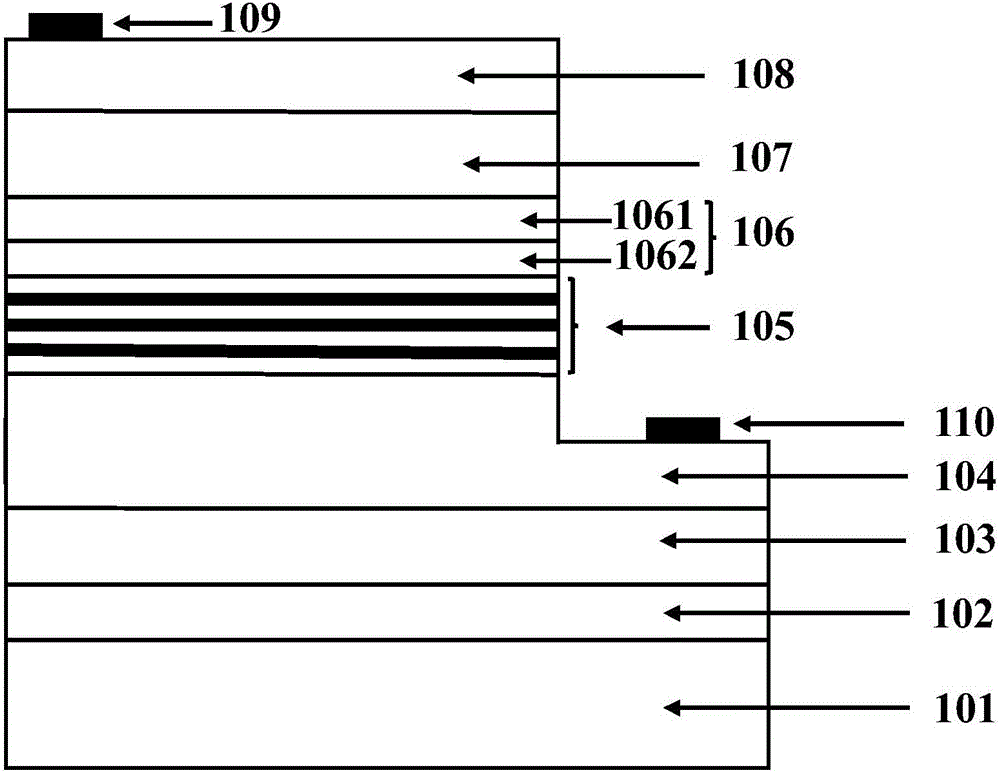
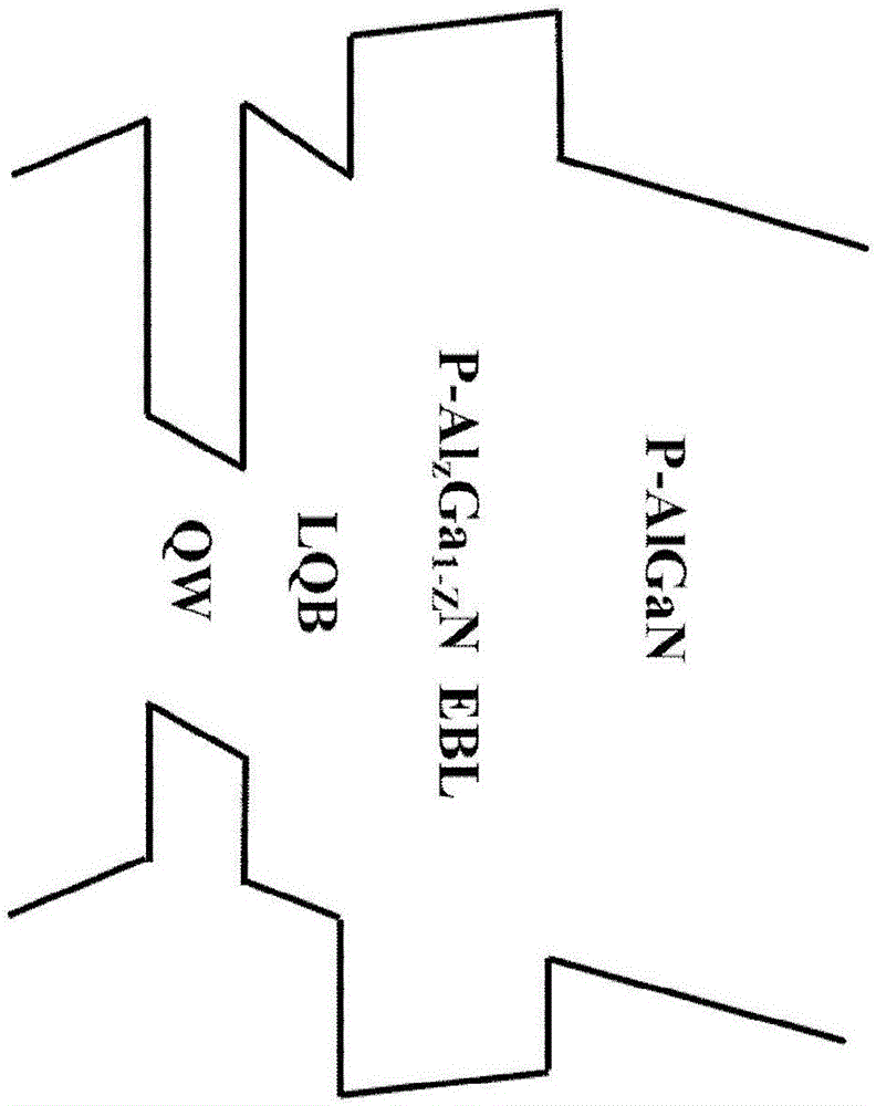
[0031] like figure 1 As shown, it is a UV-LED with a composite electron blocking layer structure provided by the present invention, including a substrate 101, a low-temperature AlN nucleation layer 102, a high-temperature AlN buffer layer 103, and an n-type AlGaN layer arranged in sequence from bottom to top 104.Al x Ga 1-x N / Al y Ga 1-y N multi-quantum well active region 105, made of p-Al s In t Ga 1-s-t N layer 1061 and p-Al z Ga 1-z N layer 1062 composed of p-Al s In t Ga 1-s-t N / p-Al z Ga 1-z N composite electron blocking layer 106, wherein z>y>x, 0≤s, t≤1, p-type AlGaN layer 107, p-type GaN ohmic contact layer 108, p-type ohmic contact layer 108 drawn on p-type GaN ohmic contact layer The electrode 109 is an n-type ohmic electrode 110 drawn out on the n-type AlGaN layer 104 .

[0032] The substrate 101 is r-plane 11-22 sapphire.

[0033] The n-type region 104 is an n-AlGaN epitaxial layer with a thickness of 1.5 μm, the n-type doping is doped with Si eleme...


PUM


Abstract

The invention discloses a UV light emitting diode with a compound electronic barrier layer structure. The light emitting diode, successively from the bottom to the top, includes a substrate (101), a low-temperature AlN nucleation layer (102), a high-temperature AlN buffer layer (103), an n type AlGaN layer (104), an Al<x>Ga<1-x>N / Al<y>Ga<1-y>N multi-quantum well active region (105), and a p-AlsIntGa1-s-tN / p-AlzGa1-zN compound electronic barrier layer (106) consisting of a p-Al<s>In<t>Ga<1-s-t> layer (106) and a p-Al<z>Ga<1-z>N layer. The diode provided can solve the problem that a conventional electronic barrier layer structure generates a parasitic electronic inversion layer between the last quantum well barrier and an electronic barrier layer.

Description

technical field [0001] The invention relates to the field of semiconductor optoelectronic devices, in particular to an ultraviolet light emitting diode (UV-LED) with a compound electron blocking layer structure. Background technique [0002] UV-LEDs based on III-nitride wide bandgap semiconductor materials have broad application prospects in the fields of sterilization and disinfection, polymer curing, biochemical detection, non-line-of-sight communication, and special lighting. Compared with the traditional ultraviolet light source mercury lamp, UV-LED has many advantages such as mercury-free environmental protection, compact and portable, low power consumption and low voltage. [0003] For AlGaN-based UV-LEDs, the asymmetric electron and hole concentrations will cause the electrons injected into the active region to easily overflow to the p-type region, reducing the effective recombination luminescence in the quantum well and causing long-wave parasitic recombination in th...

Claims


Application Information

Patent Timeline
Patent Type & Authority Applications(China)
IPC IPC(8): H01L33/14
CPCH01L33/145
Inventor 张雄梁宗文崔一平
Owner SOUTHEAST UNIV
Why Eureka
Eureka Blog
Learn More