Plasma processing device and manufacturing method thereof

A plasma and processing device technology, which is applied in the field of plasma processing devices, can solve problems such as cracking and peeling of the protective layer, poor protection ability of the protective layer, and poor processing quality of the plasma processing device, and achieve the effect of reducing manufacturing costs

Active Publication Date: 2016-10-05
ADVANCED MICRO FAB EQUIP INC CHINA
View PDF5 Cites 8 Cited by
  • Summary
  • Abstract
  • Description
  • Claims
  • Application Information

AI Technical Summary

Problems solved by technology

[0005] However, due to the large difference in thermal expansion coefficient between the internal components of the plasma processing device and the protective layer, the thermal expansion of the volume of the aluminum alloy internal components will induce cracking and peeling of the surface protective layer during the plasma etching process, resulting in The protection ability of the protective layer formed on the surface of the internal components of the plasma processing device in the prior art is poor, which still causes the problem of poor processing quality of the plasma processing device

Method used


Image

  • Plasma processing device and manufacturing method thereof
  • Plasma processing device and manufacturing method thereof
  • Plasma processing device and manufacturing method thereof

Examples


Embodiment Construction

[0057] As mentioned in the background, the protective layer formed on the surface of the internal components of the plasma processing device in the prior art has poor protection ability, which still causes the problem of poor processing quality of the plasma processing device.

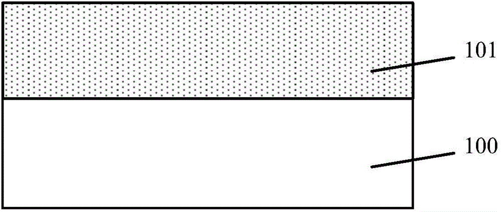
[0058] Please refer to figure 1 , figure 1 is a schematic cross-sectional structure diagram of a plasma processing apparatus according to an embodiment of the present invention. The plasma processing device includes: a substrate 100 ; and a low-density protective layer 101 located on the surface of the substrate 100 . Wherein, the substrate 100 is a shower head of a plasma processing device; the material of the low-density protective layer 101 is Y 2 o 3 .

[0059] The surface of the plasma shower head is made of silicon material or silicon carbide material, and the substrate 100 can be made of the silicon material or silicon carbide material as a whole, or coated with silicon material or silicon c...


PUM


Abstract

The invention relates to a plasma processing device and a manufacturing method thereof. The plasma processing device comprises at least one part exposed out of plasma; and the part comprises a basic body, a first protection layer and a second protection layer, wherein the first protection layer is positioned in the surface of the basic body and comprises multiple holes internally, the second protection layer is placed at the surface of the first protection layer, the density of the second protection layer is higher than that of the first protection layer, and the percentage density of the holes in the second protection layer ranges from 0 to 1%. The plasma processing device is stable in processing state, the service life is prolonged, and the capability of resisting plasma erosion is improved.

Description

technical field [0001] The invention relates to the technical field of semiconductor manufacturing, in particular to a plasma processing device and a manufacturing method thereof. Background technique [0002] Plasma treatment processes used in the manufacture of integrated circuits include plasma deposition processes, plasma etching processes, and the like. The principle of the plasma treatment process includes: using a radio frequency power source to drive a plasma generating device, such as capacitive coupled plasma (capacitive coupled plasma, CCP for short), or inductive coupled plasma (inductive coupled plasma, ICP for short)) to generate relatively The strong high-frequency alternating magnetic field makes the low-pressure reaction gas ionized to generate plasma. Plasma contains a large number of active particles such as electrons, ions, excited atoms, molecules and free radicals, which can undergo various physical and chemical reactions with the surface of the wafer ...

Claims


Application Information

Patent Timeline
Patent Type & Authority Applications(China)
IPC IPC(8): H01J37/32H01L21/00
Inventor 张力贺小明倪图强
Owner ADVANCED MICRO FAB EQUIP INC CHINA
Why Eureka
Try Eureka