
Charging method for polycrystalline silicon ingot casting process

A technology of polysilicon and ingot casting, which is applied in the charging field of polysilicon ingot casting process, which can solve the problems of excessive melting of corner and edge seeds, lower conversion efficiency of silicon wafers, and grain degradation, so as to avoid grain degradation , Avoid excessive melting and improve conversion efficiency

Inactive Publication Date: 2016-10-12
JINKO SOLAR CO LTD +1
View PDF4 Cites 9 Cited by
  • Summary
  • Abstract
  • Description
  • Claims
  • Application Information

AI Technical Summary

Problems solved by technology

[0003] However, the above-mentioned method in the prior art is relatively affected by soft felt, hard felt, thermal field structure and process. Due to the problem of thermal field structure, the silicon material at the edge will flow to the corner and edge after melting, resulting in corners Excessive melting of the top and edge seeds leads to degradation of the grains and reduces the conversion efficiency of the silicon wafer

Method used


Image

  • Charging method for polycrystalline silicon ingot casting process
  • Charging method for polycrystalline silicon ingot casting process

Examples


Embodiment Construction

[0029] The core idea of ​​the present invention is to provide a charging method for polysilicon ingot casting process, which can avoid excessive melting of corner and edge seed crystals, avoid crystal grain degradation, and improve the conversion efficiency of silicon wafers.

[0030] The following will clearly and completely describe the technical solutions in the embodiments of the present invention with reference to the accompanying drawings in the embodiments of the present invention. Obviously, the described embodiments are only some, not all, embodiments of the present invention. Based on the embodiments of the present invention, all other embodiments obtained by persons of ordinary skill in the art without making creative efforts belong to the protection scope of the present invention.

[0031] The first charging method for the polysilicon ingot process provided by the embodiment of the present application is as follows: figure 1 as shown, figure 1 It is a schematic di...


PUM

PropertyMeasurementUnit
heightaaaaaaaaaa

Abstract

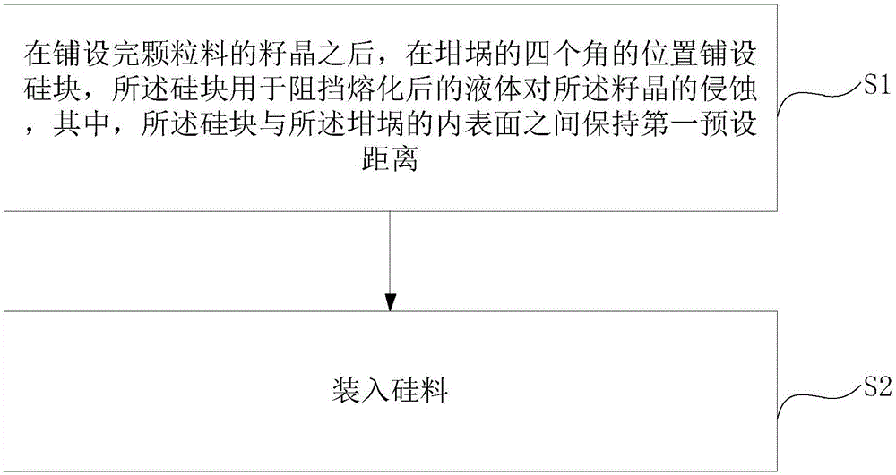
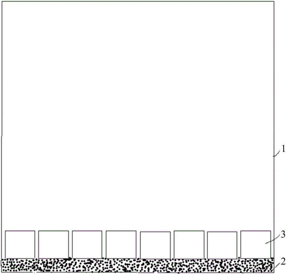
The present application discloses a charging method for polysilicon ingot casting process, which includes: after laying the seed crystal of the granular material, laying silicon blocks at the four corners of the crucible, the silicon blocks are used to block the melting after melting. erosion of the seed crystal by the liquid, wherein a first preset distance is maintained between the silicon block and the inner surface of the crucible; and silicon material is added. The above-mentioned charging method for the polysilicon ingot casting process provided by the present application can avoid too much melting of the corner and edge seed crystals, avoid crystal grain degradation, and improve the conversion efficiency of silicon wafers.

Description

technical field [0001] The invention belongs to the technical field of photovoltaic equipment, in particular to a charging method for polysilicon ingot casting process. Background technique [0002] In the polysilicon ingot casting process, the seed crystal needs to be effectively protected. The methods of protecting the seed crystal in the prior art start from the thermal field, add a layer of soft felt between the guard plate and the crucible, or add a hard felt outside the guard plate for heat insulation, and cooperate with the heat insulation cage The opening to achieve the purpose of protecting the seed crystal. [0003] However, the above-mentioned method in the prior art is relatively affected by soft felt, hard felt, thermal field structure and process. Due to the problem of thermal field structure, the silicon material at the edge will flow to the corner and edge after melting, resulting in corners Too much melting of the top and edge seeds will result in grain de...

Claims


Application Information

Patent Timeline
Patent Type & Authority Applications(China)
IPC IPC(8): C30B28/06C30B29/06
CPCC30B28/06C30B29/06
Inventor 夏宁宁李林东陈伟金浩
Owner JINKO SOLAR CO LTD
Learn More