
Baseband Chip Input Buffer Method

A baseband chip and input buffer technology, applied in the field of aircraft measurement and control, can solve the problems of complex timing design and interface interaction, affecting the correct transmission of measurement data, and high hardware stability requirements, so as to simplify interface design and interface timing, and interface timing is simple , the effect of simple structure

Active Publication Date: 2019-01-11
10TH RES INST OF CETC
View PDF5 Cites 0 Cited by
  • Summary
  • Abstract
  • Description
  • Claims
  • Application Information

AI Technical Summary

Problems solved by technology

[0003] The first is the data interaction based on the circular buffer. The application layer only needs to judge whether the input buffer of the baseband chip is full or empty, and directly input the transmission frame if it meets the conditions. This method is simple to implement, has efficient data interaction and strong Buffering ability is widely used in the communication interaction between different levels of various communication systems at present, but the disadvantage is that it has high requirements for the stability of the working environment and hardware, and it is difficult to find and recover after errors
[0004] The second is data interaction based on the ping-pong structure. Baseband processing uses two storage areas, one for reading and one for writing. The application layer detects the storage status and decides whether to write to the specified storage area. This method can achieve non-conflict interaction. It has the characteristics of good error-proof writing and recovery, but it has the characteristics of complex timing design, complex interface interaction and low adaptation rate
[0005] The first method applied to the baseband processing of the ground measurement and control station is an optimal method, but in contrast, during the flight of the aircraft, the input and output of various signals of the telemetry system are affected by the electromagnetic, vibration, acceleration, and temperature of the outside world and itself. , various interferences such as cosmic radiation have a great influence on the correct transmission of measurement data, so this method is not reliable and should not be used; while the second method is reliable, but the timing design and interface interaction are more complicated and occupy more resources. Many, especially the adaptation rate is too low is the bottleneck

Method used


Image

  • Baseband Chip Input Buffer Method
  • Baseband Chip Input Buffer Method
  • Baseband Chip Input Buffer Method

Examples


Embodiment Construction

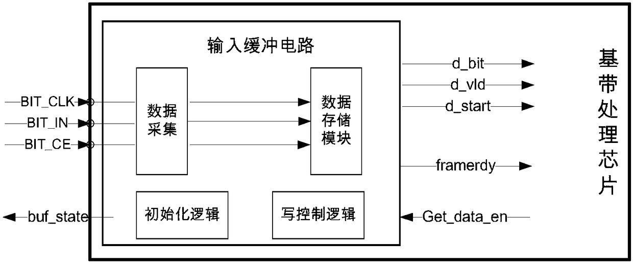
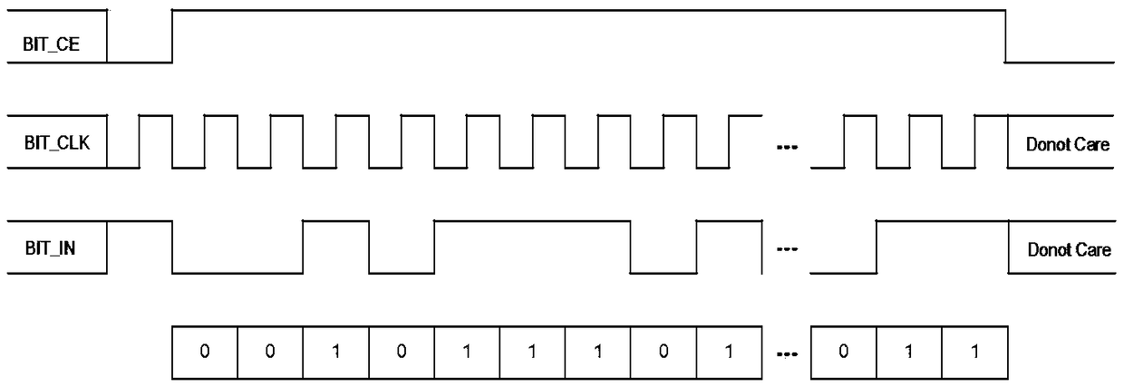
[0017] refer to figure 1 . In the embodiment described below, the input buffer circuit is provided with a data acquisition circuit, a data storage module, an initialization logic module and a write control logic module; The transmission rules are serially input to the data acquisition circuit through three single-ended lines. The data acquisition circuit detects the jump edge of the input clock by means of multi-point detection, obtains the collected data, and completes the interface processing; the collected data is pressed under the control of the write control logic module. The programming rules are written into the data storage module, and when the amount of data stored in the data storage module exceeds the preset threshold, a ready high-level indication signal is output; the subsequent processing module connected to the input buffer circuit detects the high-level indication signal, Then, according to the matching between the modulation rate and the processing rate, a re...


PUM


Abstract

The invention puts forward a baseband chip input buffer method, and aims to provide the baseband chip input buffer method which exhibit simple interface time series and high robustness and restorability. The baseband chip input buffer method is realized through the following technical scheme: a telemetering transfer frame externally input by a baseband processing chip is serially input into a data acquisition circuit through three single-ended wires according to a transmission rule of interframe dispersing and intra-frame continuity, and a clock hop edge is detected by a multipoint detection way; acquisition data is written into a data storage module according to an arrangement rule under the control of a control logic module, and a high-level index signal is output when data storage content in the data storage module exceeds a preset threshold; a later-level processing module connected with an input buffer circuit detects the high-level index signal, a request pulse is given to the input buffer circuit according to a matching situation of a modulation rate and a processing rate; and if the input buffer circuit outputs data currently, the request is not responded, and otherwise, one frame of data is read from the data storage module to be serially output according to an appointed output format.

Description

technical field [0001] The invention relates to a buffer for an aircraft baseband chip receiving input telemetry data in the field of aircraft measurement and control. Background technique [0002] In the aircraft measurement and control communication circuit, the general processing steps of aircraft telemetry data delivery are to generate telemetry data frames by the application layer, and then send them to the baseband chip for encoding according to the length of the transmission frame, and finally form a telemetry measurement frame in the baseband chip post-modulation transmission. Usually, the application layer processing and baseband processing rates do not match, and generally belong to two different hardware, so data interaction between the two layers needs to be considered. There are generally two types of interaction: [0003] The first is the data interaction based on the circular buffer. The application layer only needs to judge whether the input buffer of the b...

Claims


Application Information

Patent Timeline
Patent Type & Authority Patents(China)
IPC IPC(8): G06F13/20
CPCG06F13/20
Inventor 蒋友邦
Owner 10TH RES INST OF CETC
Learn More