Low-cost production technology of COB packaging devices

A technology for packaging devices and production processes, which is applied in semiconductor/solid-state device manufacturing, electrical components, circuits, etc., can solve the problems of high mold opening costs, low efficiency, poor flexibility, etc., and achieve easy mass production, reduce production costs, The effect of increasing the shear strength

Active Publication Date: 2016-10-12
重庆切普电子技术有限公司
View PDF11 Cites 6 Cited by
  • Summary
  • Abstract
  • Description
  • Claims
  • Application Information

AI Technical Summary

Problems solved by technology

The prior art method for producing COB packaged devices by means of a bracket has the following deficiencies: 1. The cost is high
Since the bracket is formed by mold opening, the cost of mold opening is very high, often as high as hundreds of thousands of yuan; 2. Poor flexibility
The bracket formed by mold opening has poor flexibility. Once the bracket is formed, the structure and shape will be fixed. If you want to change it, you can only open the mold again; 3. Low efficiency
Whether it is mold opening, or the installation and packaging of chips in the bracket, since the above-mentioned processing needs to be performed on each bracket separately, the efficiency will be affected

Method used


Image

  • Low-cost production technology of COB packaging devices
  • Low-cost production technology of COB packaging devices

Examples


Embodiment Construction

[0018] The present invention will be described in further detail below in conjunction with the accompanying drawings and specific embodiments.

[0019] The low-cost production process of the COB packaging device of the present invention, the steps are as follows,

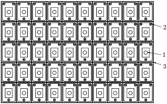
[0020] 1) According to the final dimensions of the COB packaged device to be obtained, select a PCB board of an appropriate size (the PCB board is composed of a fiber layer in the middle and copper layers on both sides), so that the PCB board can be separated from each corresponding to all COB packaged devices. packaging unit;

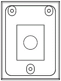
[0021] 2) According to the PCB board patterning process, the packaging unit corresponding to the COB package device to be obtained is obtained by patterning on the PCB board; any package unit and the surrounding adjacent packaging units are formed through a patterning process to facilitate subsequent cutting Cutting guide groove 3; each package unit forms a chip accommodation cavity and ele...


PUM


Abstract

The invention discloses a low-cost production technology of COB packaging devices. Various packaging units are obtained through patterning on a PCB according to a PCB patterning technology; a cutting lead groove is formed among the packaging units through the patterning technology; each packaging unit is patterned to form a chip accommodating cavity and an electrode; a chip is pasted in each chip accommodating cavity through a die bonding technology and is electrically connected with the corresponding electrode; a packaging adhesive is perfused to package the chips; and finally each packaging unit is separated through cutting along the cutting lead groove to obtain various COB packaging devices. An existing bracket is replaced with the PCB patterning technology, so that mold opening is not needed; and the production cost is greatly reduced. The PCB patterning technology is mature; mass production is easy to achieve; the production efficiency is improved; different patterns can be designed on the same PCB to obtain the devices with different sizes, structures and shapes; and personalized requirements of users are easy to achieve at low cost.

Description

technical field [0001] The invention relates to a COB packaging device, in particular to a low-cost production process of a COB packaging device, and belongs to the technical field of COB packaging. Background technique [0002] COB (chip on board) packaging is chip-on-board packaging, which is one of the bare chip mounting technologies. It is to adhere the bare chip to the interconnection substrate with conductive or non-conductive adhesive, and then perform wire bonding to realize its electrical connection. If the bare chip is directly exposed to the air, it is easy to be polluted or damaged by humans, which will affect or destroy the function of the chip, so the chip and the bonding wires are encapsulated with glue. Almost all existing COB packages use brackets, and the brackets are formed by mold opening. A cavity for accommodating chips and lead electrodes are set on the brackets. The chips are installed in the cavity by adhesive bonding and electrically connected to th...

Claims


Application Information

Patent Timeline
Patent Type & Authority Applications(China)
IPC IPC(8): H01L21/56
CPCH01L21/568
Inventor 罗安理舒斌袁杰牟维清
Owner 重庆切普电子技术有限公司
Why Eureka
Try Eureka