Check patentability & draft patents in minutes with Patsnap Eureka AI!

A kind of preparation method of oled substrate and oled substrate

A substrate and transparent substrate technology, applied in the field of OLED, can solve the problems of large non-emitting area and poor OLED display effect, and achieve the effect of increasing the pixel light-emitting area, improving the display effect, and enhancing the recognition degree.

Active Publication Date: 2019-04-23
TRULY SEMICON
View PDF3 Cites 0 Cited by
  • Summary
  • Abstract
  • Description
  • Claims
  • Application Information

AI Technical Summary

Problems solved by technology

Assuming that the alignment accuracy is △x, the theoretical maximum deviation of ITO relative to PSPI is 2△x. In order to ensure the overlap between PSPI and ITO, the design value of f must satisfy f>2△x. Similarly, in order to ensure that RIB does not Exceeding PSPI, the design value of d must satisfy d>2△x, so the OLED substrate must meet the conditions of a>c+4△x and b>e+4△x. According to this design, the area of ​​the non-luminous area is too large, The display effect of OLED is poor

Method used


Image

  • A kind of preparation method of oled substrate and oled substrate
  • A kind of preparation method of oled substrate and oled substrate
  • A kind of preparation method of oled substrate and oled substrate

Examples


Embodiment 1

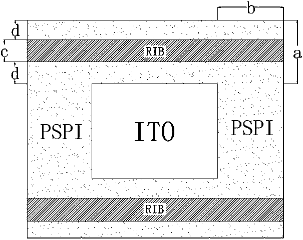
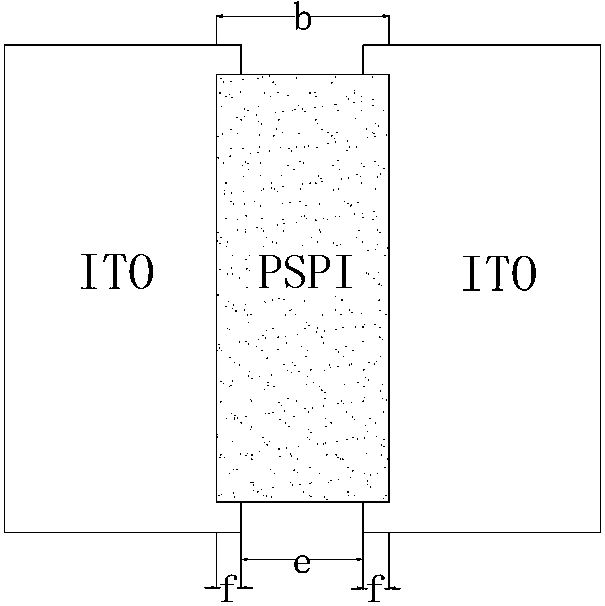
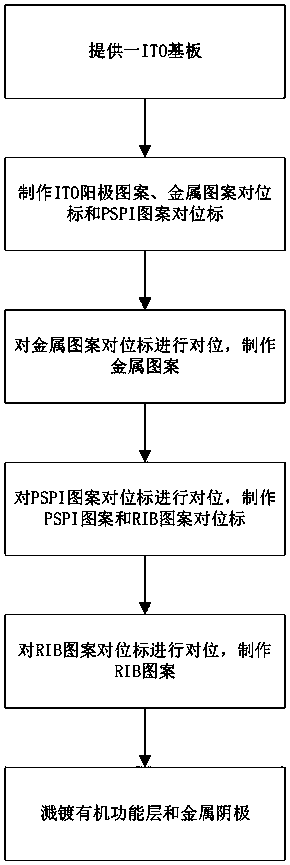
[0049] Such as image 3 Shown, a kind of preparation method of OLED substrate comprises the steps:

[0050] S1: providing an ITO substrate;

[0051] Wherein, the step S1 includes:

[0052] S1.1: Provide a transparent substrate, clean the transparent substrate, and remove dirt on the transparent substrate;

[0053] S1.2: Sputtering a layer of ITO film on the transparent substrate to form an ITO substrate;

[0054] S1.3: Planarize the ITO film to make its surface roughness Rs<1 nm.

[0055] S2: making an ITO pattern, a metal pattern alignment mark and a PSPI pattern alignment mark on the ITO substrate;

[0056] Wherein, the step S2 includes:

[0057] S2.1: coating a layer of photoresist on the ITO substrate;

[0058] S2.2: Exposing and developing the photoresist by using a mask to form a photoresist pattern;

[0059] S2.3: Produce ITO pattern, metal pattern alignment mark and PSPI alignment mark through etching process;

[0060] S2.4: Stripping off the remaining photores...

Embodiment 2

[0093] An OLED substrate, prepared by the preparation method described in Example 1.


PUM


Abstract

The invention discloses a preparation method of an OLED substrate and the OLED substrate. The metal pattern and PSPI pattern in the preparation method take the ITO pattern as the alignment reference, and the RIB pattern takes the PSPI pattern as the alignment reference. Compared with the prior art that ITO, PSPI, and RIB all use the metal pattern as the alignment reference, even if Making the width of PSPI smaller can also ensure that PSPI and ITO are overlapped, and RIB does not exceed PSPI, so that the pixel light-emitting area can be designed to increase, thereby achieving better display effects.

Description

technical field [0001] The invention relates to the field of OLEDs, in particular to a method for preparing an OLED substrate and the OLED substrate. Background technique [0002] A typical OLED pixel structure such as figure 1 with 2 As shown, PSPI isolates the ITO light-emitting area, therefore, the area of ​​the non-light-emitting area is determined by the horizontal and vertical PSPI widths. Such as figure 1 As shown, the horizontal PSPI design width a=c+2d, such as figure 2 As shown, the vertical PSPI design width b=e+2f; in actual production, c (RIB width) and e (ITO line spacing) depend on the process capability, and d and f depend on the alignment accuracy during exposure. [0003] In the existing methods for preparing OLED substrates, all the alignment marks are generally produced when the metal pattern is prepared, and the ITO pattern, PSPI pattern and RIB pattern are manufactured in sequence according to the respective alignment marks, and alignment marks are...

Claims


Application Information

Patent Timeline
Patent Type & Authority Patents(China)
IPC IPC(8): H01L27/32H01L51/52H01L51/56H01L23/544
CPCH01L23/544H01L2223/54426H10K59/00H10K50/805H10K71/00
Inventor 罗志猛赵阳峰赵云张为苍
Owner TRULY SEMICON
Features
  • R&D
  • Intellectual Property
  • Life Sciences
  • Materials
  • Tech Scout
  • Unparalleled Data Quality
  • Higher Quality Content
  • 60% Fewer Hallucinations
Learn More