Semiconductor device, inverter circuit, driving device, vehicle, and elevator

A driving device, semiconductor technology, applied in the direction of semiconductor devices, semiconductor/solid-state device manufacturing, circuits, etc., can solve problems such as inability

Active Publication Date: 2016-10-12
KK TOSHIBA
View PDF5 Cites 0 Cited by
  • Summary
  • Abstract
  • Description
  • Claims
  • Application Information

AI Technical Summary

Problems solved by technology

Therefore, there is a problem that the desired characteristics cannot be realized as SBD

Method used


Image

  • Semiconductor device, inverter circuit, driving device, vehicle, and elevator
  • Semiconductor device, inverter circuit, driving device, vehicle, and elevator
  • Semiconductor device, inverter circuit, driving device, vehicle, and elevator

Examples


no. 1 approach

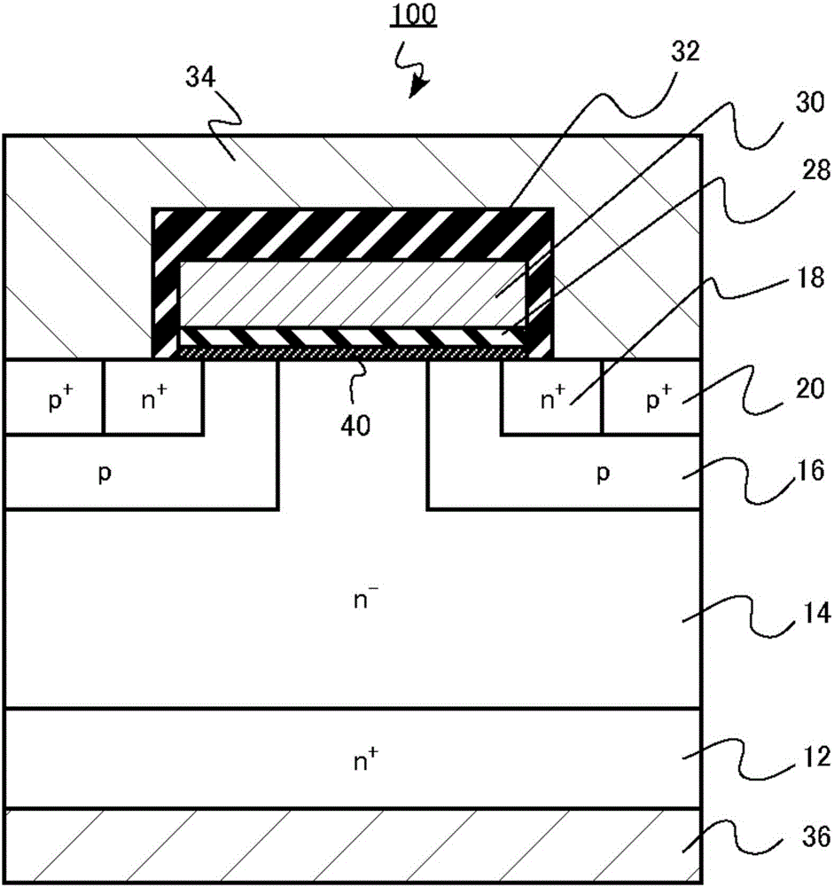
[0039] The semiconductor device of this embodiment includes: a SiC layer having a first surface; an insulating layer; a region provided between the first surface of the SiC layer and the insulating layer, the region containing Be (beryllium), Mg (magnesium), At least one element among Ca (calcium), Sr (strontium), and Ba (barium), the full width at half maximum of the concentration peak of the above-mentioned elements is 1 nm or less, when it is not combined with Si (silicon) or C on the first surface When the areal density of Si (silicon) and C (carbon) bonded to any one of (carbon) is set as the first areal density, the areal density of the above element, that is, the second areal density is 1 / of the first areal density 2 or less.

[0040] Hereinafter, for convenience, the above region is referred to as an interface region. In addition, for convenience, the above-mentioned elements contained in the interface area are referred to as terminal elements.

[0041] figure 1 It...

no. 2 approach

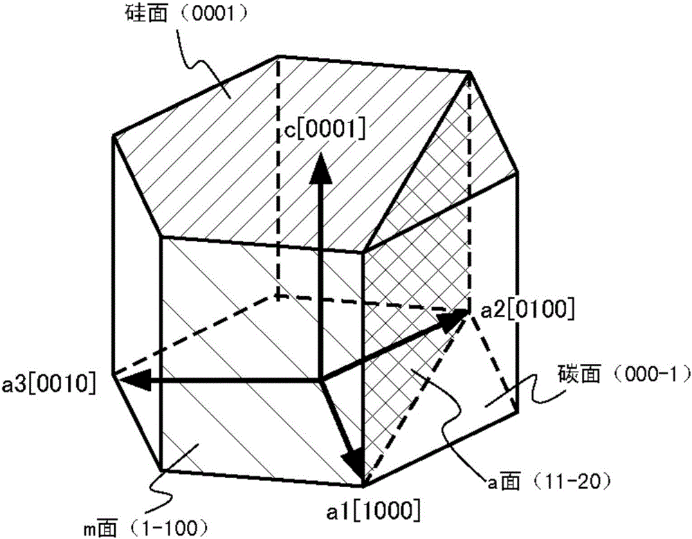
[0103] The difference between the semiconductor device of this embodiment and the first embodiment is that the surface (first surface) of the drift layer (SiC layer) is inclined from 0 to 30 degrees with respect to the carbon surface ((000-1) plane). noodle. The description of the content overlapping with the first embodiment is omitted.

[0104] The configuration of the MISFET of this embodiment is also the same as figure 1 The configuration shown is the same. Below, refer to figure 1 The MISFET of this embodiment will be described.

[0105] In the MISFET of this embodiment, the surface of the SiC substrate 12 and the surface (first surface) of the drift layer (SiC layer) 14 are inclined from 0 to 30 degrees with respect to the carbon plane ((000-1) plane). noodle.

[0106] Furthermore, an interface region 40 is provided at the interface between the drift layer (SiC layer) 14 and the gate insulating layer (insulating layer) 28 . The interface region 40 contains at least...

no. 3 approach

[0111] The difference between the semiconductor device of this embodiment and the first embodiment is that the surface (first surface) of the drift layer (SiC layer) is a surface inclined by 0° to 30° with respect to the direction. The description of the content overlapping with the first embodiment is omitted.

[0112] In the MISFET of this embodiment, the surface of the SiC substrate 12 and the surface (first surface) of the drift layer (SiC layer) 14 are surfaces inclined by 0° to 30° with respect to the direction. For example, the surface of the drift layer 14 is an a-plane or an m-plane. In addition, the notation related to the direction includes the [0001] direction and the [000-1] direction.

[0113] Furthermore, an interface region 40 is provided at the interface between the drift layer 14 and the gate insulating layer (insulating layer) 28 . The interface region 40 contains at least one element (terminal element) selected from Be (beryllium), Mg (magnesium), Ca (ca...


PUM


Abstract

A semiconductor device according to the embodiments includes a SiC layer having a first plane, an insulating layer, and a region between the first plane and the insulating layer, the region including at least one element in the group consisting of Be (beryllium), Mg (magnesium), Ca (calcium), Sr (strontium), and Ba (barium), a full width at half maximum of a concentration peak of the element being equal to or less than 1 nm, and when a first area density being an area density of Si (silicon) and C (carbon) including a bond which does not bond with any of Si and C in the SiC layer at the first plane and a second area density being an area density of the element, the second area density being equal to or less than 1 2 of the first area density.

Description

[0001] This application claims priority based on Japanese Patent Application No. 2015-061799 filed on March 24, 2015 and Japanese Patent Application No. 2015-236876 filed on December 3, 2015, the entire contents of which are incorporated herein. technical field [0002] Embodiments of the present invention relate to a semiconductor device, an inverter circuit, a drive device, a vehicle, and an elevator. Background technique [0003] SiC (silicon carbide) is expected as a material for next-generation semiconductor devices. SiC has excellent physical properties such as a band gap three times larger, a breakdown electric field strength about ten times higher, and a thermal conductivity about three times higher than Si (silicon). If this characteristic is fully utilized, it is possible to realize a low-loss semiconductor device capable of operating at a high temperature. [0004] However, for example, when SiC is used to form a MIS (Metal Insulator Semiconductor; Metal Insulato...

Claims


Application Information

Patent Timeline
Patent Type & Authority Applications(China)
IPC IPC(8): H01L29/04H01L29/06H01L29/24H01L29/78
CPCH01L29/045H01L29/06H01L29/24H01L29/7827H01L21/045H01L21/049H01L29/872H01L29/47H01L29/8613H01L29/0619H01L29/1602H01L29/66068H01L29/513H01L29/7395H01L29/7811H01L29/7813H01L29/0615H01L29/1608H01L29/7802H01L29/063H01L29/1095
Inventor 清水达雄饭岛良介
Owner KK TOSHIBA
Why Eureka
Try Eureka