Gate oxide structure and preparation method

A technology of gate oxide structure and oxide layer, which is applied in the field of semiconductors, can solve problems such as increasing the electric field at the gate oxide material, reducing tunneling current, and reliability problems, so as to improve channel mobility, improve forward conduction capability, The effect of improving reliability

Pending Publication Date: 2022-04-08
ZHEJIANG UNIV HANGZHOU GLOBAL SCI & TECH INNOVATION CENT
View PDF0 Cites 1 Cited by
  • Summary
  • Abstract
  • Description
  • Claims
  • Application Information

AI Technical Summary

Problems solved by technology

[0002] SiC-based power devices benefit from the superior physical properties of SiC materials such as wide bandgap, high breakdown field strength, and high thermal conductivity. The field has great prospects. In the preparation process of SiC power devices, especially Metal-Oxide-Semiconductor Field-Effect Transistors (Metal-Oxide-Semiconductor Field-Effect Transistors, MOSFETs), lower quality gate interface oxides have greatly limited Performance of power devices
[0003] The gate oxide used in the current stage is often SiO 2 materials, which are usually grown by direct thermal oxidation of SiC, but for thermal oxygen grown SiO 2 layer, more interface defects will inevitably appear at the interface, resulting in a sharp drop in channel mobility, which is far from the theoretical electron mobility of SiC. In addition, due to SiO 2 The dielectric constant is only 3.9, which will increase the electric field at the gate oxide material, which poses a big problem for its reliability
[0004] as SiO 2 material substitution to Al 2 o 3 , HfO 2 Gate oxide materials represented by high dielectric constant materials have been widely studied in recent years. However, compared with SiO 2 , the bandgap width is often narrow, so that under the action of the gate voltage, due to the matching of the high dielectric constant material and SiC, the gap between the conduction band and the valence band is small, so that electrons can easily cross the potential barrier, resulting in a larger Large tunneling current, resulting in large energy loss at the gate
[0005] On the other hand, the traditional gate oxide structure by SiO 2 Set Al on 2 o 3 layer, although it can further widen the carrier barrier at the gate oxide, thereby reducing the tunneling current, but due to Al 2 o 3 There are many crystal phases in the material, and in the process of heating and cooling, various crystal phase structures will transform each other, and it is easy to produce grain boundaries, so that under the action of the gate voltage, the Al 2 o 3 The material is prone to gate leakage current, and then it is easy to break down under high field strength, resulting in great difficulties in practical applications

Method used


Image

  • Gate oxide structure and preparation method
  • Gate oxide structure and preparation method
  • Gate oxide structure and preparation method

Examples


Embodiment 1

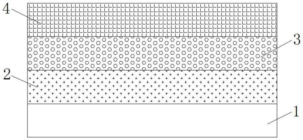
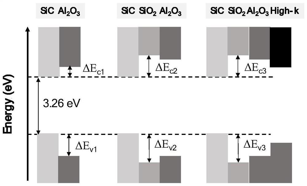
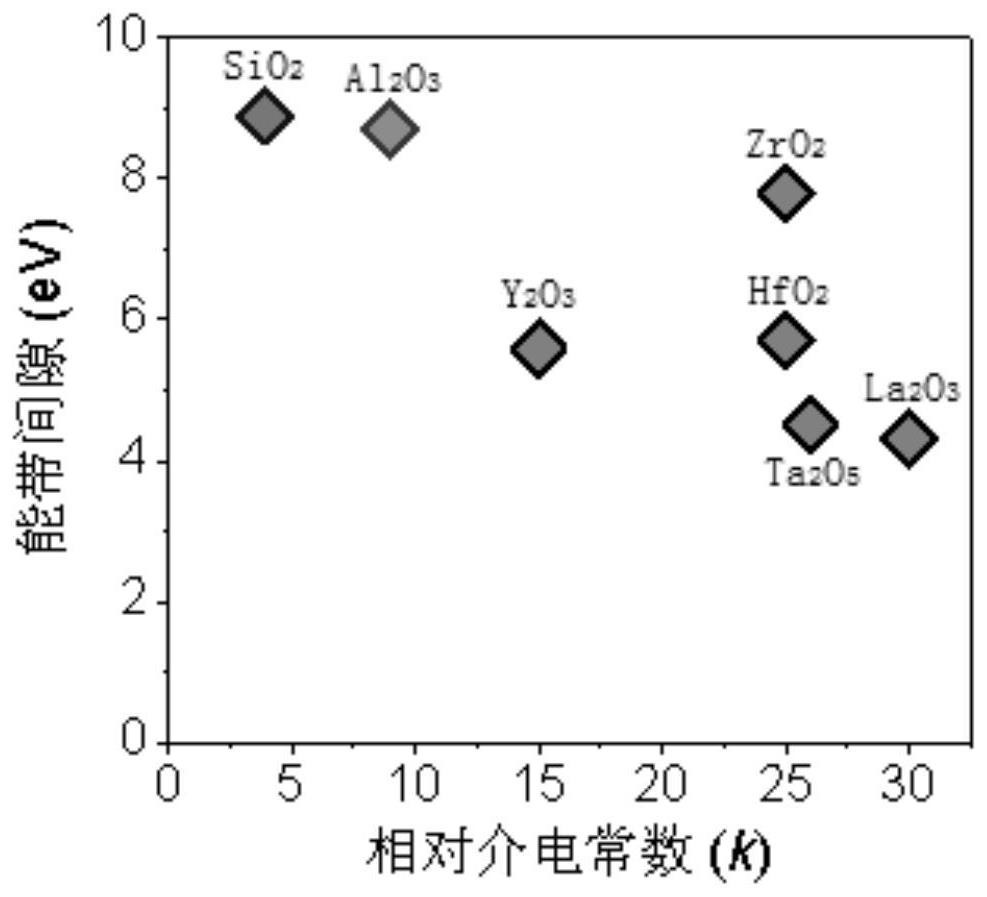
[0032] A gate oxide structure comprising a SiC substrate layer 1, an oxide layer 2, an intermediate layer 3 and a high dielectric material layer 4, the oxide layer 2 is disposed on the SiC substrate layer 1, the intermediate layer 3 is disposed on the oxide layer 2, and the intermediate layer 3 The side away from the oxide layer 2 is provided with a high dielectric material layer 4, and the high dielectric material layer 4 is HfO 2 layer, ZrO 2 Layer or Y 2 o 3 Any one of the layers, the middle layer 3 is Al 2 o 3 layer.

[0033] The traditional gate oxide structure uses SiO 2 Only one layer of Al is added on the layer 2 o 3 layer, but due to Al 2 o 3 The dielectric constant is 9, and the bandgap is 8.7eV, which has both high dielectric constant and bandgap, but due to Al 2 o 3 There are many crystal phases, and in the process of heating and cooling, various crystal phase structures will be converted to each other, and grain boundaries are easily generated, which le...

Embodiment 2

[0040] A method for preparing a gate oxide structure, comprising the following steps: using a cleaning gas to clean surface crystal plane defects of a SiC substrate layer 1 at 500°C, wherein the cleaning gas can be hydrogen; Oxidize the cleaned SiC substrate layer 1 in an oxygen environment at 1500°C to obtain an oxide layer 2, namely SiO 2 layer, while controlling the generated SiO by oxidation time 2 The thickness of the layer; the method of high temperature annealing is used to eliminate the surface dangling bond passivation and interface state defects of the oxide layer 2, wherein the annealing temperature for eliminating the surface dangling bond passivation and interface state defects of the oxide layer 2 is 1350 ° C, and the oxide layer The atmospheric pressure of dangling bond passivation and interface state defects on the surface of 2 is 1.5 Pa, and the atmosphere environment for eliminating the surface dangling bond passivation and interface state defects of oxide la...

Embodiment 3

[0046] In this embodiment, the high dielectric material is also HfO 2 The material is used as an example to describe the preparation process, but the difference between this embodiment and the second embodiment is that the HfO 2 materials were deposited to obtain HfO 2 layer, its obtained thickness is 30nm, and the deposition time of controlled low-pressure vapor deposition at this time is 2 hours.


PUM

PropertyMeasurementUnit
thicknessaaaaaaaaaa
thicknessaaaaaaaaaa
thicknessaaaaaaaaaa

Abstract

The invention relates to a gate oxide structure and a preparation method in the technical field of semiconductors, the gate oxide structure comprises a SiC substrate layer, an oxide layer, an Al2O3 layer and a high dielectric material layer, the oxide layer is arranged on the SiC substrate layer of the gate oxide structure and the preparation method, the Al2O3 layer is arranged on the oxide layer of the gate oxide structure and the preparation method, and the high dielectric material layer is arranged on the high dielectric material layer. According to the gate-oxide structure and the preparation method, the high-dielectric material layer is arranged on one side, far away from the oxide layer, of the Al2O3 layer, so that the gate-oxide structure has the advantages of high channel mobility and small gate energy loss, and breaks through the bottleneck that the gate of the traditional gate-oxide structure is easy to leak current.

Description

technical field [0001] The present application relates to the field of semiconductor technology, in particular to a gate oxide structure and a preparation method. Background technique [0002] SiC-based power devices benefit from the superior physical properties of SiC materials such as wide bandgap, high breakdown field strength, and high thermal conductivity. The field has great prospects. In the preparation process of SiC power devices, especially Metal-Oxide-Semiconductor Field-Effect Transistors (Metal-Oxide-Semiconductor Field-Effect Transistors, MOSFETs), lower quality gate interface oxides have greatly limited performance of power devices. [0003] The gate oxide used in the current stage is often SiO 2 materials, which are usually grown by direct thermal oxidation of SiC, but for thermal oxygen grown SiO 2 layer, more interface defects will inevitably appear at the interface, resulting in a sharp drop in channel mobility, which is far from the theoretical electro...

Claims


Application Information

Patent Timeline
Patent Type & Authority Applications(China)
IPC IPC(8): H01L29/51C23C14/08C23C16/40C23C16/455C23C16/56C23C28/04H01L21/28
Inventor 盛况邵泽伟王珩宇任娜
Owner ZHEJIANG UNIV HANGZHOU GLOBAL SCI & TECH INNOVATION CENT
Why Eureka
Try Eureka