TN (tunnel nitrate)-SONOS (silicon oxide nitrate oxide silicon) memory with composite nitrogen-based dielectric tunneling layer

A TN-SONOS, composite medium technology, applied in the direction of semiconductor devices, electrical solid devices, electrical components, etc., can solve the problem of not being able to simultaneously meet the data writing and erasing speed and data static retention characteristics, and the silicon nitride storage layer is resistant to erasing and writing. The ability and data retention ability are reduced, and it is difficult to meet the requirements of the speed of data writing and erasing, so as to improve the data retention characteristics, reduce traps and interface states, and improve the erasing rate and operation window.

Inactive Publication Date: 2012-12-12
EAST CHINA NORMAL UNIV +1
View PDF5 Cites 0 Cited by
  • Summary
  • Abstract
  • Description
  • Claims
  • Application Information

AI Technical Summary

Problems solved by technology

With the continuous development of memory technology, in order to make the erasing speed reach the practical application, the thickness of the tunnel oxide layer must be less than 30? Retention capability will be reduced, thereby affecting the reliability of the memory
If a thicker tunneling layer is used, the large electric field required for the erasing operation will cause electrons to be injected from the gate through the barrier layer into the charge trapping layer, and the injection of gate electrons will neutralize the injection of holes, resulting in erase In addition to saturation, if the erase saturation is too large, the erasure of charges cannot be achieved at all
Therefore, the tunneling layer of traditional SONOS is gradually unable to meet the contradictory requirements of data writing and erasing speed and data static retention characteristics at the same time: because the tunneling layer is thick with silicon dioxide, it is difficult to meet the requirements for data writing and erasing speed. Thin tunneling layer silicon dioxide is difficult to meet the requirements for data static retention characteristics

Method used


Image

  • TN (tunnel nitrate)-SONOS (silicon oxide nitrate oxide silicon) memory with composite nitrogen-based dielectric tunneling layer
  • TN (tunnel nitrate)-SONOS (silicon oxide nitrate oxide silicon) memory with composite nitrogen-based dielectric tunneling layer
  • TN (tunnel nitrate)-SONOS (silicon oxide nitrate oxide silicon) memory with composite nitrogen-based dielectric tunneling layer

Examples


Embodiment 1

[0028] This embodiment provides a specific manufacturing method of the memory of the present invention.

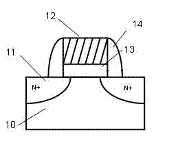
[0029]Firstly, a semiconductor substrate is provided, and then a layer of SiON is formed by dry oxygen oxidation on the substrate in an atmosphere containing nitrogen. (x) , where the value of x is 1.25, and the layer thickness is 13?. Then use LPCVD on SiON (x) A layer of Si is formed on top 3 N 4 , a thickness of 20?. Then use LPCVD technique on Si 3 N 4 SiON (y) , where the value of y is 1.65 and the thickness is 35?. After the tunneling layer is formed, LPCVD technology is used to form 60? Si 3 N 4 Charge trapping layer and 60? SiO2 blocking layer. Then a polysilicon gate is formed on it by LPCVD, and side wall structures are formed on both sides of the gate. Finally, source and drain regions are formed by self-aligned ion implantation.

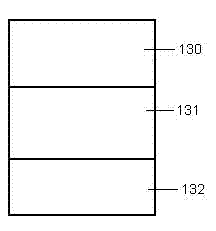
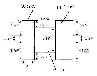
[0030] image 3 Shown is a schematic diagram of the energy bands of the dielectric stack between the gate and channel...


PUM


Abstract

The invention relates to the field of semiconductor memories, and discloses a TN (tunnel nitrate)-SONOS (silicon oxide nitrate oxide silicon) memory with a composite nitrogen-based dielectric tunneling layer. The TN-SONOS memory comprises a semiconductor substrate, a grid electrode and a dielectric laminate; the semiconductor substrate comprises a channel, a source terminal and a drain terminal, and the source terminal and the drain terminal are adjacent to the channel; the dielectric laminate is arranged between the grid electrode and the surface of the channel and comprises a tunneling layer, a charge trapping layer and a stopping layer, the tunneling layer is in contact with the surface of the channel, the charge trapping layer is laminated on the upper side of the tunneling layer, and the stopping layer is laminated on the upper side of the charge trapping layer and is in contact with the grid electrode; and the tunneling layer is the composite dielectric tunneling layer and comprises a first layer consisting of silicon oxynitride SiON(x), a second layer consisting of Si3N4 and a third layer consisting of silicon oxynitride, SiON(y), the first layer is in contact with the surface of the channel, the second layer is adjacent to the first layer, and the third layer is adjacent to the second layer. By the TN-SONOS memory, the performance of a SONOS nonvolatile memory is improved, and the TN-SONOS memory can be applied to extremely small memory devices with high quality.

Description

technical field [0001] The invention relates to the field of semiconductor memory, in particular to a TN-SONOS memory with a composite nitrogen-based dielectric tunneling layer. Background technique [0002] In the field of semiconductor memory, flash memory is a kind of non-volatile memory technology. Traditional flash memory uses floating gates as charge storage units. However, with the continuous development of flash memory technology, the storage density continues to increase, and the distance between floating gates If it is reduced, there will be mutual influence between the stored charges of adjacent floating gates, which hinders the increase of storage density for floating gate flash memory technology. The SONOS (silicon-silicon dioxide-silicon nitride-silicon dioxide-silicon) memory uses an insulating charge trapping layer to replace the floating gate, completely avoiding the interaction between the stored charges, and it also has its unique The ONO structure makes ...

Claims


Application Information

Patent Timeline
Patent Type & Authority Applications(China)
IPC IPC(8): H01L27/115H01L29/792H01L29/51
Inventor 石艳玲张顺斌刘丽娟曹刚陈广龙沈国飞陈赞栋周群李曦
Owner EAST CHINA NORMAL UNIV
Why Eureka
Try Eureka