Substrate holder and method for growing monocrystalline diamond
A technology of microwave plasma and chemical vapor phase, applied in chemical instruments and methods, crystal growth, from chemically reactive gases, etc.
- Summary
- Abstract
- Description
- Claims
- Application Information
AI Technical Summary
Problems solved by technology
Method used
Image
Examples
Embodiment 1
[0026] Example 1. Growth of high-quality single crystal diamond using a newly designed grooved substrate stage
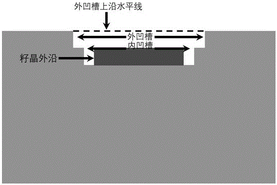
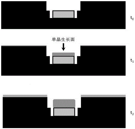
[0027] Step 1: During the implementation process, we designed a series of molybdenum substrate stages with series grooves (see figure 2 ). The grooves of any one of the substrate tables are formed by nesting inner grooves and outer grooves. The inner groove is a square structure with dimensions (a+0.2) mm x (a+0.2) mm, where a is the width of the diamond seed (in this example, 4 mm). The outer groove is a square structure with dimensions (a+0.4) mm x (a+0.4) mm. There is a step between the inner groove and the outer groove, the width of the step is 0.2 mm, and the height of the step (that is, the depth of the inner groove) is 0.5 mm smaller than the depth of the outer groove. The difference between different substrate stages in the whole series is that the total depth of their grooves is different, and the depth from the smallest to the largest is 0.5mm, 1.0mm, ...
Embodiment 2
[0033] Example 2. Growth using a common substrate platform (comparison).
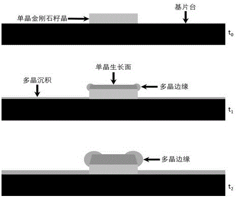
[0034] The ordinary molybdenum substrate stage is used for growth, and the controlled growth conditions are exactly the same as the growth conditions of the new groove substrate stage (reaction chamber pressure, microwave power, seed crystal size used), that is, except that the sample stage is an ordinary molybdenum substrate stage In addition, the above-mentioned steps 2, 3 and 4 were also carried out. After about 24 hours of growth, it was found that the surface of the diamond single crystal was extremely uneven, and the growth rate around it was much higher than that in the middle. Due to the uneven surface temperature and the different deposition rates of C atoms , resulting in polycrystalline and some amorphous carbon at the edges (see Figure 4 ).
PUM
| Property | Measurement | Unit |
|---|---|---|
| thickness | aaaaa | aaaaa |
| depth | aaaaa | aaaaa |
| size | aaaaa | aaaaa |
Abstract
Description
Claims
Application Information


