Pico-second superfast electrical property testing system for semiconductor device

A technology of electrical characteristics and semiconductors, which is applied in the field of electrical parameter extraction of semiconductor devices, can solve problems such as inability to fully reflect the transport of carriers and defects, and achieve the effect of ensuring integrity

Active Publication Date: 2016-10-26
ZHEJIANG UNIV
View PDF3 Cites 9 Cited by
  • Summary
  • Abstract
  • Description
  • Claims
  • Application Information

AI Technical Summary

Problems solved by technology

The fastest Rapid I currently reported D -V G In the test method, the rising and falling edges are several nanoseconds, which cannot fully reflect the transport movement between carriers and defects

Method used


Image

  • Pico-second superfast electrical property testing system for semiconductor device
  • Pico-second superfast electrical property testing system for semiconductor device
  • Pico-second superfast electrical property testing system for semiconductor device

Examples


Embodiment Construction

[0018] The technical solution of the present invention will be described in detail below in conjunction with the accompanying drawings and specific embodiments.

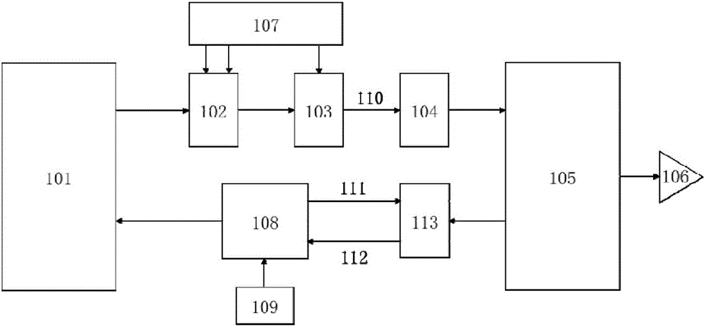
[0019] Such as figure 1 As shown, this embodiment is a picosecond-level ultra-fast electrical characteristic testing system applied to semiconductor devices, including a waveform processor 101, a broadband voltage amplifier 102, a broadband voltage bias device 103, and a broadband pick-up tee device 108 , the first microwave probe 104 , and the second microwave probe 113 . The waveform processor 101 generates a voltage pulse waveform whose rising edge and falling edge are less than 100pS or a voltage signal 110 of a pseudo-random binary code sequence voltage waveform, which is sequentially transmitted from the output channel to the broadband voltage amplifier 102 and the broadband voltage biaser 103 , the gate voltage signal 110 is loaded on the gate of the MOSFET transistor 105 to be tested through the first microw...


PUM


Abstract

The invention discloses a pico-second superfast electrical property testing system for a semiconductor device. The system is composed of a waveform processor, a broadband voltage amplifier, a broadband voltage bias device, a broadband pick-up three-way device, a first microwave probe and a second microwave probe. The system is characterized in that a pico-second pulse sequence waveform is applied to an electronic device, so that the electronic device is in an actual working environment like a CPU and thus electrical characteristics of the electronic device in the CPU at a practical switching speed of a 100-pS level are tested. The system is applied to electrical characteristic researches of a high-performance planar transistor using silicon, germanium or an III-V-group compound as a carrier subchannel and a fin type three-dimensional gate structure type or GAA structure type field effect transistor.

Description

technical field [0001] The invention belongs to the field of extraction of electrical parameters of semiconductor devices, in particular to a method for extracting high-performance electronic devices, especially metal oxide semiconductor field-effect transistors (MOSFETs) devices in a very short time (100pS). D -V G test method. Background technique [0002] In the past few decades, with the development of CMOS integrated circuit technology, the size of the core unit in the circuit - metal oxide semiconductor field effect transistors (MOSFETs) has gradually decreased in accordance with Moore's law, from a few microns (μm) to 14nm , The density and performance of transistor devices continue to increase. As the gate length continues to shrink, the thickness of the oxide layer continues to decrease, the junction depth of the device decreases, and the threshold voltage decreases, the performance of MOSFET transistor devices will be affected by factors such as mobility degradat...

Claims


Application Information

Patent Timeline
Patent Type & Authority Applications(China)
IPC IPC(8): G01R31/26
CPCG01R31/2621
Inventor 赵毅张睿卢继武曲益明
Owner ZHEJIANG UNIV
Why Eureka
Try Eureka