
Microcomponent transfer method and device, and electronic equipment

A transfer method and technology of micro-components, applied in the direction of electrical components, circuits, and electric solid-state devices, etc., can solve the problems of performance degradation of micro-components, thermal budget limitation, etc.

Inactive Publication Date: 2016-10-26
XIAMEN SANAN OPTOELECTRONICS TECH CO LTD
View PDF4 Cites 33 Cited by
  • Summary
  • Abstract
  • Description
  • Claims
  • Application Information

AI Technical Summary

Problems solved by technology

In addition, in the fabrication process using transfer head arrays, the thermal budget of microcomponents for phase change is limited, usually less than 350 °C, or more specifically, less than 200 °C; otherwise, the performance of microcomponents will be degraded

Method used


Image

  • Microcomponent transfer method and device, and electronic equipment
  • Microcomponent transfer method and device, and electronic equipment
  • Microcomponent transfer method and device, and electronic equipment

Examples


Embodiment 1

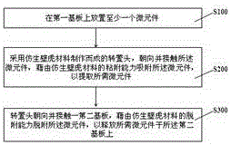
[0034] figure 1 A method for transferring micro components is shown, which mainly includes process steps S100~S300, combined below Figure 2~8 Be explained.

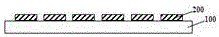
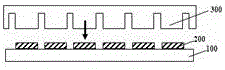
[0035] Such as figure 2 As shown, a first substrate 100 is provided, which can be a growth substrate or a carrier substrate. The carrier substrate is preferred in this embodiment, and the material of the carrier substrate can be glass, silicon, polycarbonate (Polycarbonate, PC), acrylonitrile-butadiene Acrylonitrile Butadiene Styrene (ABS) or any combination thereof. It should be understood that the specific implementations of the carrier substrate mentioned above are only examples, and are not intended to limit the present invention. Those skilled in the art of the present invention should flexibly choose the specific implementation of the first substrate 100 according to actual needs. Way. Several micro-elements 200 are placed on the first substrate 100. The micro-elements may be wafers or light-emitting diodes or...

Embodiment 2

[0042] Such as Figure 9 As shown, the difference from Example 1 is that the micro-element described in Embodiment 1 is a light-emitting diode that has been subjected to a wafer dicing process, while the micro-element 200 of this embodiment is a wafer that has not been subjected to a wafer dicing process. The circle includes chip area 210 and scribe line area 220 . Since the transpose head made of bionic gecko material has a strong adsorption effect on micro-components, the transpose head does not need to be made to match the size or shape of the wafer, so that the transpose head 300 can be fully utilized. Adaptability without special processing.

Embodiment 3

[0044] Such as Figure 10 As shown, taking a display screen with a size of 138.1mm*67mm as an example, it has 1334×750 two-dimensional array micro-pitch RGB three-color LED chips, in which the horizontal line width (X) of the LED chip is 103 μm, and the vertical line width (Y) is 89 μm, the lateral dimension (X) of the LED chip is 93 μm, the longitudinal dimension (Y) is 80 μm, the lateral spacing (X) is 10 μm, and the longitudinal spacing (Y) is 9 μm; the lateral line width of the LED chip (X) = Lateral size of LED chip (X) + Lateral spacing (X); Lateral line width of LED chip (Y) = Lateral size of LED chip (Y) + Lateral spacing (Y).

[0045] Such as Figure 11~12 As shown, the upper surface of the two-dimensional array micro-pitch RGB three-color LED chip uses transparent electrodes (such as ITO) as wires to realize the electrical connection of each LED chip to avoid light absorption or shading; the lower surface of the RGB three-color LED chip can be set ITO or sapphire (...


PUM


Abstract

The invention discloses a microcomponent transfer method and device, and electronic equipment. The method comprises the steps: putting at least one microcomponents on a first substrate; enabling a transfer head made of a biomimetic gecko material to face and contact with the microcomponents, and absorbing the microcomponents through the adhesive capability of the biomimetic gecko material, so as to extract the needed microcomponents; enabling the transfer head to face a second substrate, and desorbing the microcomponents through the desorption capability of the biomimetic gecko material, so as to release the needed microcomponents on the second substrate.

Description

technical field [0001] The present invention relates to microcomponents for display, and more particularly, to a transfer method for microcomponents, a microcomponent device, and an electronic device including the microcomponent device. Background technique [0002] Micro-component technology refers to an array of micro-sized components integrated at high density on a substrate. At present, micro-pitch light-emitting diode (Micro LED) technology has gradually become a research hotspot, and the industry expects high-quality micro-component products to enter the market. High-quality fine-pitch light-emitting diode products will have a profound impact on traditional display products such as LCD / OLED that are already on the market. [0003] In the process of fabricating microcomponents, the microcomponents are first formed on a donor substrate and then transferred to a receiving substrate. The receiving substrate is, for example, a display screen. One difficulty in the fabric...

Claims


Application Information

Patent Timeline
Patent Type & Authority Applications(China)
IPC IPC(8): H01L21/683H01L33/00
CPCH01L21/6835H01L33/0093H01L2221/68318H01L2221/68354H01L2221/68381H01L21/683H01L33/00
Inventor 徐宸科郑建森邵小娟林科闯
Owner XIAMEN SANAN OPTOELECTRONICS TECH CO LTD
Learn More