Array substrate and preparation method thereof, display panel, and display device

A technology for array substrates and display panels, applied in static indicators, semiconductor/solid-state device manufacturing, instruments, etc., can solve the problems of reducing the side frame of the gate drive, reducing the side frame of the gateIC, etc., to reduce the difficulty of drilling , reduce complexity, reduce the effect of width

Active Publication Date: 2016-10-26
BOE TECH GRP CO LTD +1
View PDF4 Cites 23 Cited by
  • Summary
  • Abstract
  • Description
  • Claims
  • Application Information

AI Technical Summary

Problems solved by technology

[0003] In the prior art, the array substrate row-driven GOA (gate on array) structure can effectively reduce the width of the gate drive side frame, and even if the display device adopts the GOA structure, the gate fanout line still needs to be drawn from the edge of the substrate. Traces, there is a limitation on the width of the traces, making it impossible to reduce the gate IC side frame infinitely

Method used


Image

  • Array substrate and preparation method thereof, display panel, and display device
  • Array substrate and preparation method thereof, display panel, and display device
  • Array substrate and preparation method thereof, display panel, and display device

Examples


preparation example Construction

[0045] The invention also discloses a method for preparing an array substrate, the method comprising:

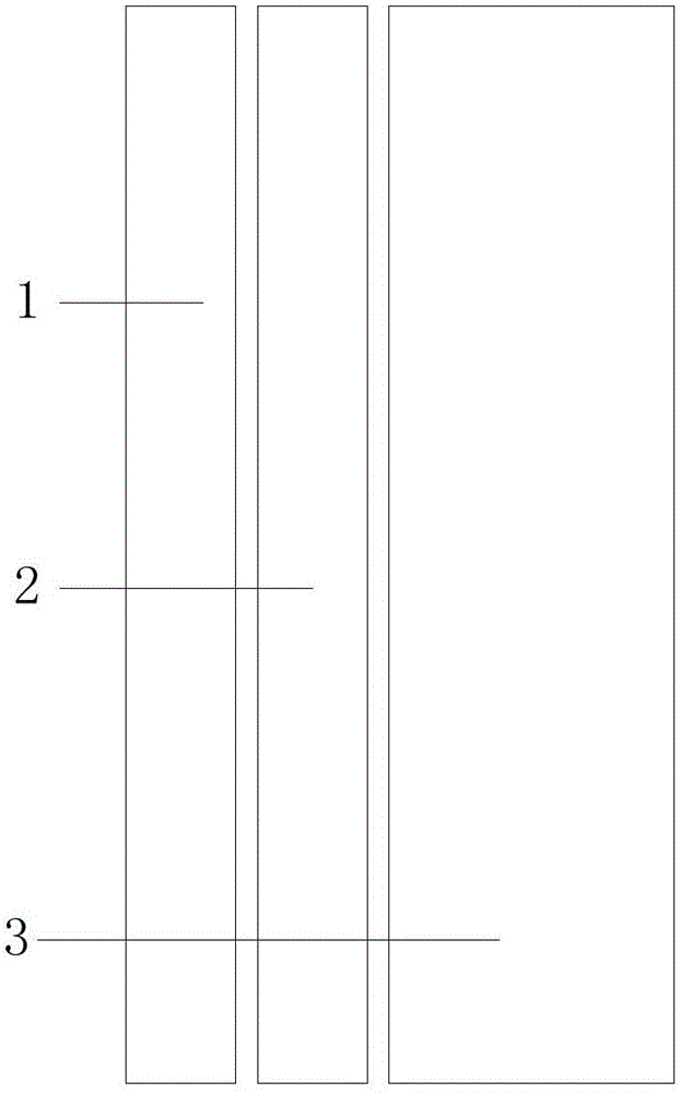
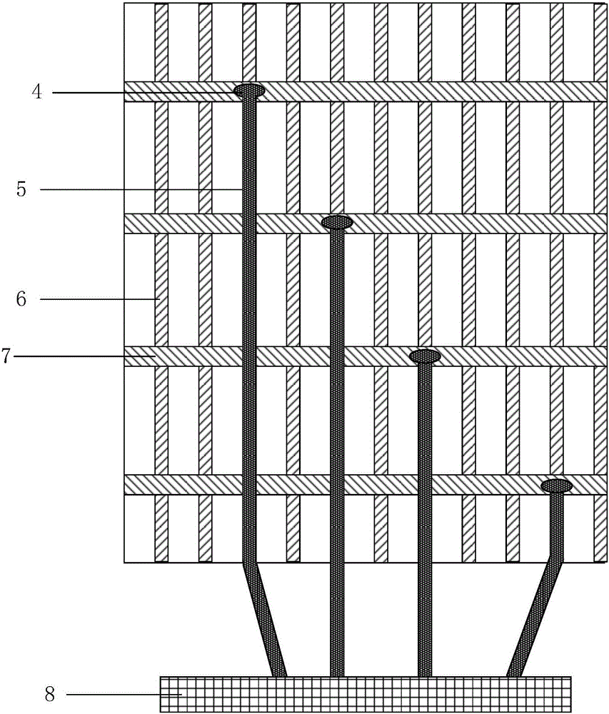
[0046] S1. Form via holes on a substrate with gate lines, data lines, and gate fan-out lines formed on one side; wherein the via holes are arranged in the projection area of ​​the gate lines on the substrate;

[0047] S2. Form a gate fan-out line on the side of the substrate that is away from the gate line, so that the gate fan-out line is connected to the gate of the array substrate through a via hole; the gate fan-out line is routed along the black matrix projection area and extends to the driver binding area.

[0048] In the above method, the gate fan-out line is arranged on the side of the substrate that is away from the gate line, and the line is routed along the projection area of ​​the black matrix and extended to the driving bonding area, so that the gate fan-out line does not go along the side of the array substrate, thereby reducing the The width of the gate drivi...

Embodiment 1

[0059] The method of the present embodiment comprises the following steps:

[0060] S11. Manufacturing openings on the TFT glass substrate by one etching or laser drilling method, the openings are arranged in the first black matrix projection area gate BM corresponding to the grid line area of ​​the substrate and the second black matrix corresponding to the data line area. Intersection of matrix projection area Source BM. The etching method in this step may be Dry Etch, Wet Etch or RIE etc.

[0061] S12. Deposit a conductive material in the opening by means of electroplating, physical vapor deposition PVD or chemical vapor deposition CVD. The conductive material can be metal, conductive semiconductor or conductive plastic.

[0062] S13 , removing the protruding conductive material through chemical mechanical polishing (CMP) to make the back surface of the TFT glass substrate flat.

[0063] S14. Manufacture a gate fanout line gatefanout on the back of the TFT glass substrate ...

Embodiment 2

[0073] The method of the present embodiment comprises the following steps:

[0074] S21. Making openings on the TFT glass by etching twice or laser drilling, the openings are at the junction of the gate BM and the Source BM. The etching method in this step may be Dry Etch, Wet Etch or RIE etc.

[0075] S22. Deposit a conductive material in the opening by means of electroplating, PVD, CVD, etc. The conductive material can be metal, conductive semiconductor or conductive plastic.

[0076] S23 , removing the protruding conductive material by CMP, so that the back surface of the TFT glass substrate is flat.

[0077] S24. Manufacture a gate fanout on the back of the TFT glass substrate by photolithography→thin film deposition→etching. The fanout line is along the BM projection direction and communicates with the conductive material of the opening.

[0078] S25 , depositing a protective layer for gate fanout.

[0079] The difference between the method of this embodiment and the m...


PUM


Abstract

The present invention discloses an array substrate and a preparation method thereof, a display panel, and a display device. A grid fan-out line is arranged on one side of a substrate departing from the grid line, goes line along a black matrix projection area and extends to a driving binding area so as to allow the grid fan-out line not to go the side of the array substrate and reduce the width of the grid driving side frame, and because the grid fan-out line goes line on the projection area on the array substrate along the black matrix, the display effect of the array substrate cannot be influenced. Compared to the punching area of the punching technical scheme in a driving binding area in the prior art, the punching area of the technical scheme of punching in the display area and leading out the grid fan-out line from the back surface of the substrate is increased, and the array substrate and the preparation method thereof, the display panel, and the display device can punch fewer holes in a certain range compared to the technical scheme in the prior art, and therefore the difficulty of punching is reduced, the complexity of the preparation technology is reduced, and the preparation efficiency is improved.

Description

technical field [0001] The invention relates to the field of preparation of liquid crystal displays, and more specifically relates to an array substrate and a preparation method thereof, a display panel, and a display device. Background technique [0002] The side frame of the gate drive gate IC of a traditional display device, that is, the part from the display area AA to the edge of the array substrate TFT usually includes 3 parts, such as figure 1 Shown: drive fanout line part 3 (that is, IC fanout (including the sealing area)), drive part 2 (that is, IC part) IC, and part 1 from the drive part to the edge of the substrate (that is, the part from IC to the edge of TFT). Since the trace width of IC fanout part 3 is usually 4-7mm, plus the width of IC part 2 is 0.6mm, and the distance from IC to part 1 of TFT edge is 0.6mm, the gate IC side frame is usually 5-8mm, which hinders The bezels are getting narrower. [0003] In the prior art, the array substrate row-driven GOA ...

Claims


Application Information

Patent Timeline
Patent Type & Authority Applications(China)
IPC IPC(8): H01L27/12H01L21/77G02F1/133G02F1/1362
CPCG02F1/133G02F1/1362H01L21/77H01L27/1214H01L27/124H01L2021/775
Inventor 金硕董学邱云黄小妹王锡彬王志东
Owner BOE TECH GRP CO LTD
Why Eureka
Try Eureka