Epitaxial wafer manufacturing method and epitaxial wafer

A technology of epitaxial wafers and manufacturing methods, applied in semiconductor/solid-state device manufacturing, electrical components, circuits, etc., can solve problems such as uncaptured gettering regions, poor crystallinity of wafer surfaces, and epitaxial layer defects, etc., to achieve excellent absorption effect of suppressing the formation of epitaxial defects

Active Publication Date: 2016-10-26
SUMCO CORP
View PDF6 Cites 4 Cited by
  • Summary
  • Abstract
  • Description
  • Claims
  • Application Information

AI Technical Summary

Problems solved by technology

[0008] However, when an epitaxial layer is formed on a silicon wafer or when a device element is formed on a device formation region, if contaminating metals adhere to the wafer surface, the contaminating metals cannot be detached from the device formation region due to the lowering of the temperature of the device formation process described above. May not be trapped into gettering regions that exist deep from the wafer surface
[0009] In addition, in order to form a gettering layer by implanting carbon ions at a high concentration at a position deep from the wafer surface, the accelerating voltage of the carbon ions must be increased. defect problem

Method used


Image

  • Epitaxial wafer manufacturing method and epitaxial wafer
  • Epitaxial wafer manufacturing method and epitaxial wafer
  • Epitaxial wafer manufacturing method and epitaxial wafer

Examples


Embodiment

[0069] (Invention Example 1-Invention Example 3)

[0070] Examples of the present invention will be described below.

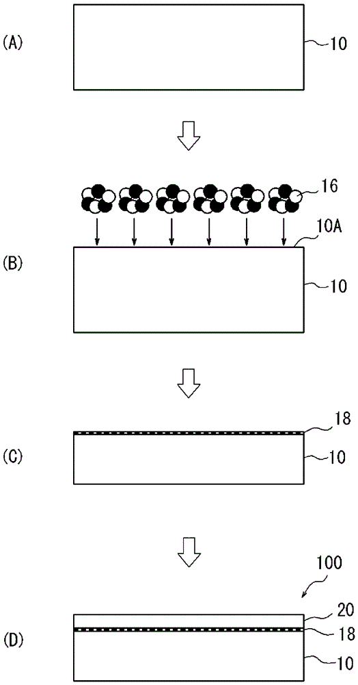
[0071] First, as a substrate of an epitaxial wafer, a silicon wafer having a diameter of 300 mm, a thickness of 775 μm, and a resistivity of about 0.003 Ω·cm was prepared. Next, using a cluster ion generator (manufactured by Nisshin Ion Machinery Co., Ltd., model: CLARIS), generate C 3 h 5 The clusters were irradiated on the surface of the silicon wafer as cluster ions under the condition that the acceleration voltage per carbon atom was 23.4 keV / atom. Here, the dose of cluster ions is 1.0×10 15 atom / cm 2 (Invention Example 1), 5×10 15 atom / cm 2 (Invention Example 2), 2×10 14 atom / cm 2 (invention example 3) these three levels. Next, the silicon wafer was transported to a monolithic epitaxial growth apparatus (manufactured by Applied Materials, Inc.), and hydrogen baking was performed at a temperature of 1120° C. for 30 seconds in the apparatus. The...


PUM

PropertyMeasurementUnit
electrical resistivityaaaaaaaaaa
diameteraaaaaaaaaa

Abstract

Provided is a method for manufacturing an epitaxial wafer which has excellent gettering capability while suppressing the formation of epitaxial defects. This method is characterized by involving: a cluster ion irradiation step in which cluster ions (16), which contain at least carbon, are irradiated in a dose amount of 2.0*1014 / cm2 to 1.0*1016 / cm2 onto the surface of a silicon wafer (10) having a resistivity of 0.001-0.1 omega*cm, and a modified layer (18) consisting of a solid solution of the constituent elements of the cluster ions (16) is formed on the surface of the silicon wafer (10); and a epitaxial layer forming step in which an epitaxial layer (20) having higher resistivity than the silicon wafer (10) is formed on the modified layer (18) of the silicon wafer (10).

Description

technical field [0001] The present invention relates to a manufacturing method of an epitaxial wafer and an epitaxial wafer, in particular to a manufacturing method of an epitaxial wafer that suppresses the formation of epitaxial defects and has excellent gettering capability. Background technique [0002] In recent years, the miniaturization of silicon devices has been progressing, and it is required that there be no crystal defects in the device formation region that increase the leakage current and shorten the lifetime of the carrier. In order to meet this requirement, an epitaxial wafer is manufactured in which an epitaxial layer is grown on a silicon wafer, and the epitaxial layer on the surface is used as a device formation region. [0003] One of the problems in the silicon device manufacturing process is the contamination of heavy metals into the wafer. For example, when heavy metals such as cobalt, copper, or nickel are mixed into the wafer, it will cause poor dwel...

Claims


Application Information

Patent Timeline
Patent Type & Authority Applications(China)
IPC IPC(8): H01L21/322H01L21/20H01L21/265
CPCH01L21/26506H01L21/26566H01L21/3221H01L21/02381H01L21/02447H01L21/02532H01L21/0262H01L21/02658H01L21/02694H01L29/36
Inventor 岩永卓朗栗田一成门野武
Owner SUMCO CORP
Why Eureka
Try Eureka