Method for manufacturing selective emitter solar cell from local laser melting phosphorosilicate glass

A phosphosilicate glass and laser melting technology, applied in laser welding equipment, circuits, electrical components, etc., can solve the problems of open circuit voltage, short circuit current drop, affecting battery performance, etc. simple effect

Active Publication Date: 2012-08-22
HANWHA SOLARONE QIDONG
View PDF7 Cites 0 Cited by
  • Summary
  • Abstract
  • Description
  • Claims
  • Application Information

AI Technical Summary

Problems solved by technology

Under such high surface concentration and junction depth conditions, extremely high emission recombination will lead to a significant drop in open circuit voltage and short circuit current, seriously affecting battery performance

Method used


Image

  • Method for manufacturing selective emitter solar cell from local laser melting phosphorosilicate glass
  • Method for manufacturing selective emitter solar cell from local laser melting phosphorosilicate glass
  • Method for manufacturing selective emitter solar cell from local laser melting phosphorosilicate glass

Examples


Embodiment Construction

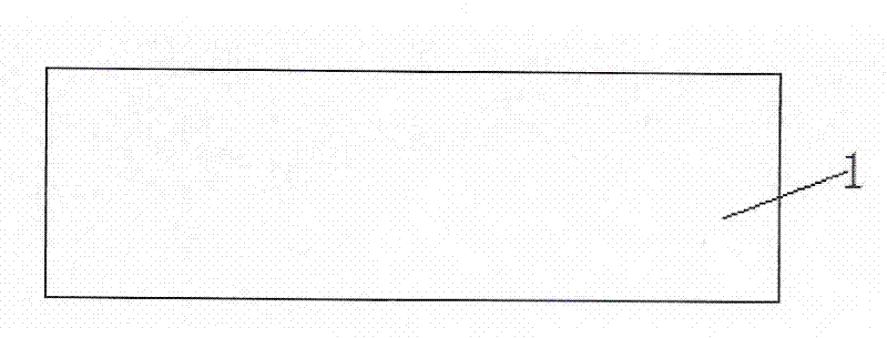
[0029] refer to figure 1 , the first step is to clean wafer 1, remove the surface damage layer, and texture the surface: for single crystal, use 5% NaOH alkaline solution for pyramid texturing; for polycrystalline, use 1:5 (weight ratio) hydrogen An aqueous solution of hydrofluoric acid and nitric acid is used for isotropic texturing.

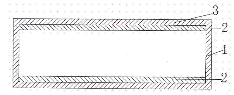
[0030] refer to figure 2 , the second step is to use a tube furnace for phosphorus diffusion (or online diffusion method) to form an n-type layer 2 with a square resistance of 80Ω / □, and at the same time generate phosphosilicate glass 3 with a thickness of 80nm on the surface, and the phosphorus in the phosphosilicate glass The content is adjusted by the amount of phosphorus source introduced during the diffusion process, and the thickness of phosphosilicate glass is adjusted by the amount of oxygen introduced during the diffusion process;

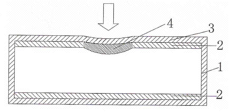
[0031] refer to image 3 , the third step uses the Q switch Nd:YVO 4 The 532nm wavelength laser s...


PUM

PropertyMeasurementUnit
thicknessaaaaaaaaaa
thicknessaaaaaaaaaa

Abstract

The invention discloses a method for manufacturing a selective emitter solar cell from local laser melting phosphorosilicate glass, which comprises the following steps of: texturing the surface of a chip; performing phosphorous diffusion by utilizing thermal diffusion, and generating the phosphorosilicate glass on the surface; diffusing the phosphorous element in the phosphorosilicate glass on a laser scanning part into the chip through local chip-melting; isolating the boundary; removing a damaged layer formed in the laser chip-melting process; removing the residual phosphorosilicate glass; forming a coating on the front surface; plating silver paste on the front surface of the chip in a screen printing mode, and obtaining a front electrode in a laser scanned area; plating the silver paste on a rear surface of the chip to form a back electrode, and plating aluminum paste on the rear surface of the chip in the screen printing mode to form a back electric field; and sintering the chip to make the metal electrode element and silicon in the chip eutectic. Only one diffusion process is present in the whole process, and the process is simple, has no damage to the silicon chip and has good gettering effect.

Description

technical field [0001] The invention relates to a method of making a selective emitter solar cell. Background technique [0002] New energy is one of the five most decisive technological fields in the world economic development in the 21st century. Solar energy is a clean, efficient and inexhaustible new energy source. In the new century, the governments of various countries regard the utilization of solar energy resources as an important content of the national sustainable development strategy. Photovoltaic power generation has the advantages of safety, reliability, no noise, no pollution, less constraints, low failure rate, and easy maintenance. In recent years, with the rapid development of international photovoltaic power generation, the supply of solar chips is in short supply, so improving the photoelectric conversion efficiency of solar chips and the production capacity of solar chips has become an important issue. [0003] The conventional process uniform emitter ...

Claims


Application Information

Patent Timeline
Patent Type & Authority Patents(China)
IPC IPC(8): H01L31/18B41M1/12B23K26/00
CPCY02P70/50
Inventor 魏青竹马跃陈文浚穆汉
Owner HANWHA SOLARONE QIDONG
Why Eureka
Try Eureka