

Semiconductor monocrystalline silicon multi-wire cutting clamping device and method
A multi-wire cutting and clamping device technology, applied in fine working devices, working accessories, stone processing equipment and other directions, can solve the problem of uneven thickness of silicon wafers, reduce the deviation of slice thickness, solve the problem of uneven thickness of silicon wafers, The effect of good application value
- Summary
- Abstract
- Description
- Claims
- Application Information
AI Technical Summary
Problems solved by technology
Method used
Image

Examples
Embodiment 1
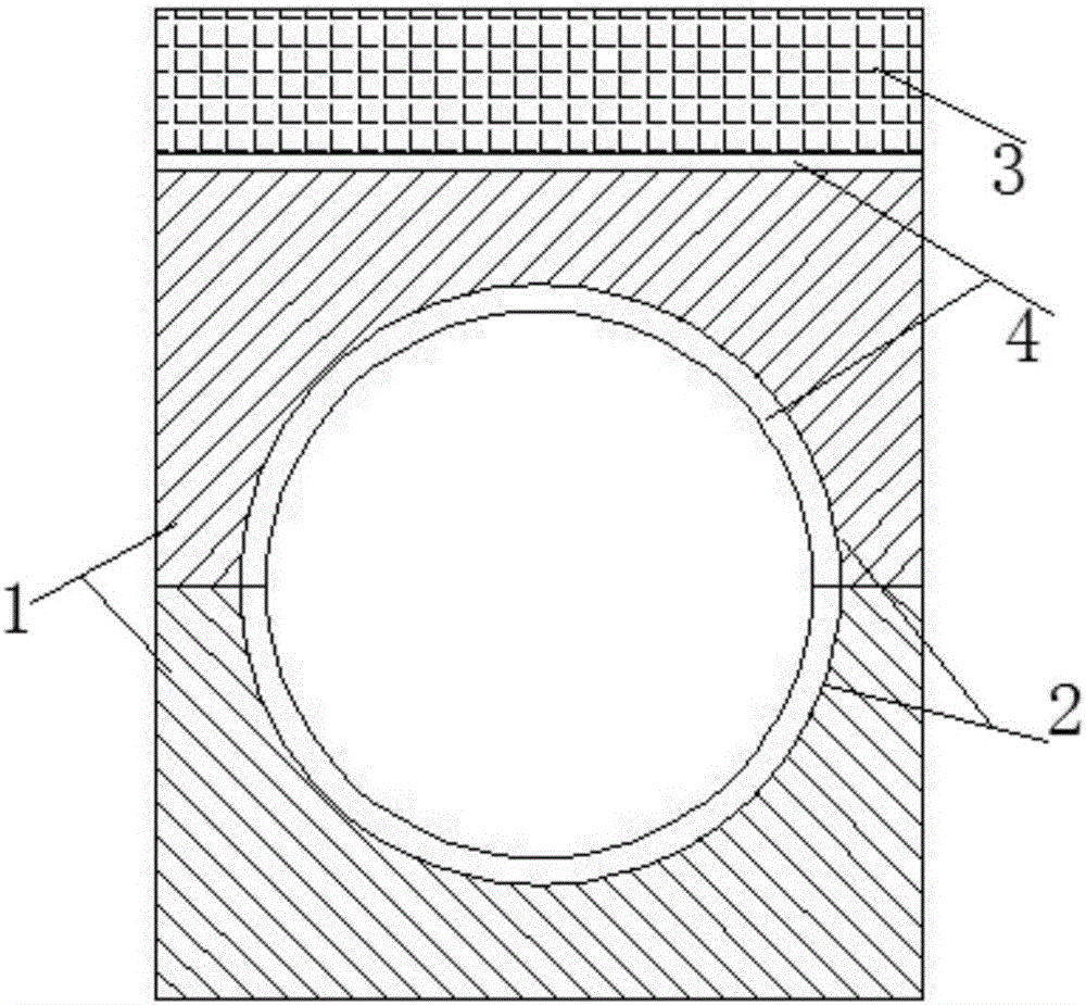
[0031] Processing of N-type 4-inch crystal ingot, with main reference surface, slice thickness 580 microns, asymmetric chamfering, used for energy-saving lamp power triode substrate production, processed according to conventional multi-wire cutting, the total thickness change is 14.3 microns . Such as figure 1 Shown, adopt the inventive method to process, and step is as follows:
[0032] According to the production demand, the surface of the corresponding ingot will be tumbled and processed, and the surface of the monocrystalline silicon ingot will be cleaned for cutting;
[0033] Carry out the crystal orientation test on the crystal orientation instrument, and make a mark. Use two splints 1 of resin material, place the silicon rod in the groove 2 inside the splint 1, and the arc length of the groove 2 inside the splint 1 is equal. is 4 inches, the width of splint 1 is 110mm,
[0034] Adhesive 4, which is epoxy resin AB glue, is used to bond the groove 2 to the silicon rod...
Embodiment 2
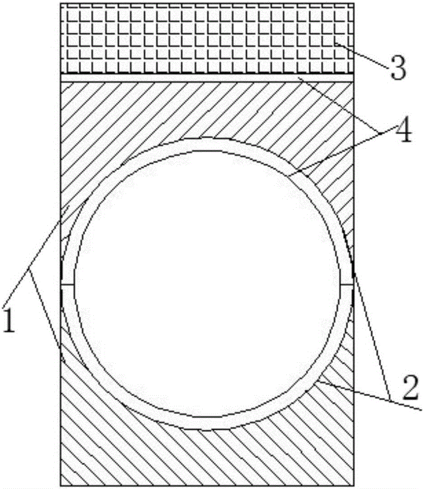
[0039] Processing N-type 6-inch ingot, with main reference surface, slice thickness 340 microns, symmetrical chamfering, used for bridge stack diode core substrate production, processed according to conventional multi-wire cutting, the total thickness change is 18.1 microns. Such as figure 2 Shown, adopt the inventive method to process, and step is as follows:
[0040] According to the production demand, the surface of the corresponding ingot will be tumbled and processed, and the surface of the monocrystalline silicon ingot will be cleaned for cutting;
[0041] Carry out the crystal orientation test on the crystal orientation instrument, and make a mark. Use two splints 1 of resin material, place the silicon rod in the groove 2 inside the splint 1, and the arc length of the groove 2 inside the splint 1 is equal. is 6 inches, the width of splint 1 is 156mm,
[0042] Adhesive 4, which is epoxy resin AB glue, is used to bond the groove 2 to the silicon rod, and place it for ...
Embodiment 3
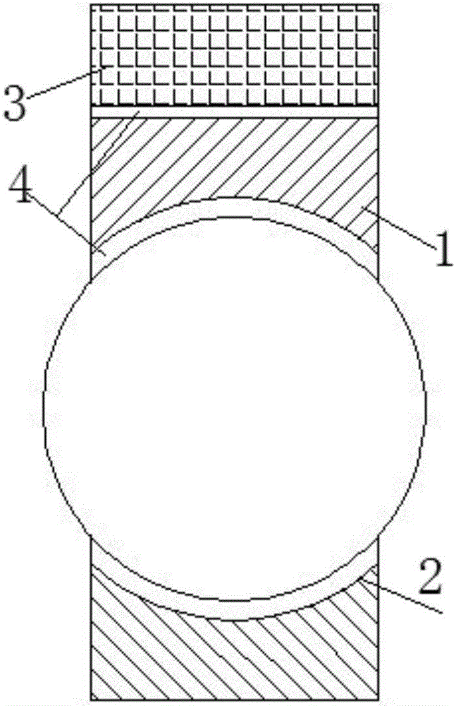
[0047] Processing N-type 5-inch ingot, with main reference surface, slice thickness 400 microns, symmetrical chamfering, used for TVS diode core substrate production, processed according to conventional multi-wire cutting, the total thickness change is 15.5 microns. Such as image 3 Shown, adopt the inventive method to process, and step is as follows:
[0048] According to the production demand, the surface of the corresponding ingot will be tumbled and processed, and the surface of the monocrystalline silicon ingot will be cleaned for cutting;
[0049] Carry out the crystal orientation test on the crystal orientation instrument, and make a mark. Use two splints 1 of resin material, place the silicon rod in the groove 2 inside the splint 1, and the arc length of the groove 2 inside the splint 1 is equal. is 5 inches, the width of splint 1 is 100mm,
[0050] Adhesive 4, which is epoxy resin AB glue, is used to bond the groove 2 to the silicon rod, and place it for 10-20 minu...
PUM
 Abstract
Description
Claims
Application Information