A multi-bridge connection, small-pitch edge-wrapped printed circuit board and its manufacturing method

A technology for printed circuit boards and manufacturing methods, which is applied in the directions of printed circuit components, electrical connection printed components, and the formation of electrical connections of printed components, etc., and can solve the problem of edge-wrapping copper skin warping, too small bridge connection, poor milling defects, etc. Problems, to achieve the effect of good bonding force of gold-clad board edge, prevent warping and falling off, and enhance the bonding force of gold-clad

Active Publication Date: 2018-07-13
HUIZHOU KING BROTHER CIRCUIT TECH +2
View PDF5 Cites 0 Cited by
  • Summary
  • Abstract
  • Description
  • Claims
  • Application Information

AI Technical Summary

Problems solved by technology

[0003] However, with the continuous development of circuit board products, customers have more and more diversified and strict requirements for the gold-clad edge of circuit boards, and the corresponding product sizes are getting smaller and smaller, resulting in smaller and smaller bridges. When metal Intermediate spacing between bit and metal bit: 1mm≤minimum spacing≤2mm, after milling and reaming, the bridging width is only 0.2mm to 1.2mm, and the conventional process (such as figure 1 ) Milling the half-side holes after tinning will cause the bridge connection to be too small and disconnected, and the board cannot be fixed and manufactured; if the half-side holes are not milled after the tinning, it will cause the edge-wrapping copper skin to warp and poor milling in subsequent molding, which will greatly It affects the production quality and product quality of the hemming, and also affects the installation and use of customer products
[0004] How to control the quality of the product's edge wrapping, prevent the edge wrapping copper from lifting and milling, and meet the production requirements of the minimum distance between the metal position and the metal position of 1mm to 2mm, has always been a difficult problem in the machining process, which greatly affects the electrical properties of the product. performance and appearance

Method used


Image

  • A multi-bridge connection, small-pitch edge-wrapped printed circuit board and its manufacturing method
  • A multi-bridge connection, small-pitch edge-wrapped printed circuit board and its manufacturing method
  • A multi-bridge connection, small-pitch edge-wrapped printed circuit board and its manufacturing method

Examples


Embodiment 1

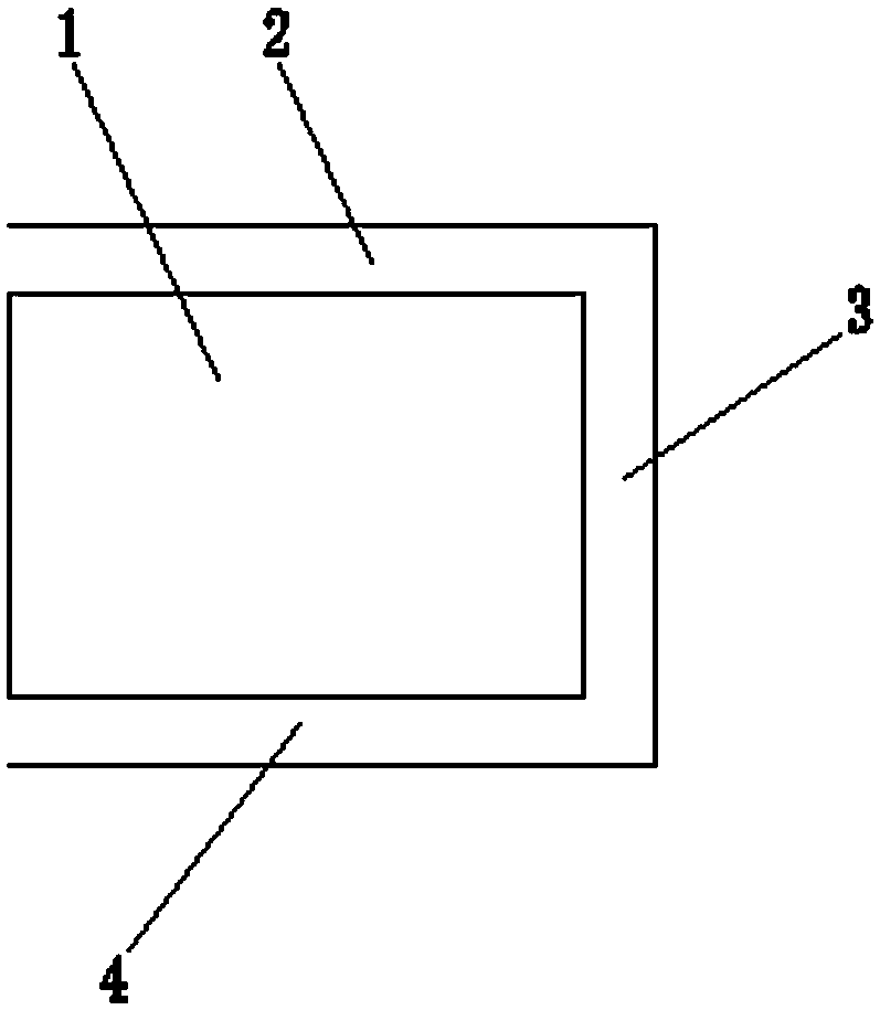
[0042]Such as figure 1 As shown, a printed circuit board with multi-bridge connection and small-pitch edging is mainly composed of a circuit board 1, the side of the circuit board 1 is provided with a metal edging 3, and the upper end surface of the metal edging 3 is connected to the top The surface graphics 2 are connected, and the lower end surface of the metal wrapping 3 is connected with the bottom surface graphics 4. The present invention connects the upper end surface of the metal edging 3 with the top surface graphic 2, and the edging design of the connection between the lower end surface of the metal edging 3 and the bottom surface graphic 4 can effectively enhance the binding force of the plate edge gold coating and prevent the edge edging during the forming process. The copper skin is lifted, falling off, etc., to ensure that the drill bit is in clockwise contact with the wrapping when drilling, effectively ensuring that the drill bit does not lift the copper belt wh...

Embodiment 2

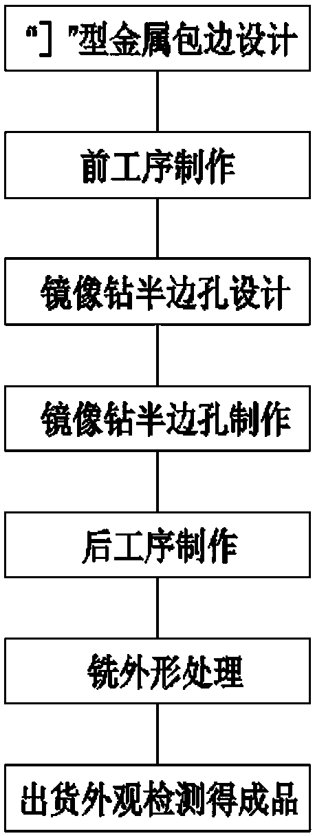
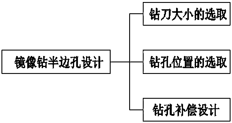
[0044] The structure and principle of this embodiment and embodiment 2 are basically the same, the difference is: as figure 2 As shown, when the upper end surface and the lower end surface of the metal edging 3 are not connected with the top figure 2 and the bottom figure 4, the metal edging 3 is designed as a "]" type metal edging 3 (such as image 3 shown), when the metal edging 3 is a "]" type metal edging 3, the distance between the "]" type metal edging 3 and the circuit pattern is greater than or equal to 3mil. When the metal edging 3 is a "]" type metal edging 3, the length of the edging corners 5 at the top and bottom of the "]" type metal edging 3 is greater than or equal to 3 mils, which effectively ensures the stability of the edging and prevents the edging fall off. The multi-bridge connection and small-pitch edge-wrapping printed circuit board of the present invention adopts the design of "]" type metal edge wrapping 3, which can effectively enhance the bonding ...


PUM


Abstract

Disclosed is a multi-bridging position and small-spacing edge-wrapped printed circuit board, which is mainly composed of a circuit plate (1). A side face of the circuit plate (1) is provided with a metal wrapping edge (3). The metal wrapping edge (3) is "]"-shaped, or the upper end face of the metal wrapping edge (3) is connected to a top face pattern (2) and the lower end face of the metal wrapping edge (3) is connected to a bottom face pattern (4). Further disclosed is a manufacturing method for the multi-bridging position and small-spacing edge-wrapped printed circuit board, comprising the following steps: a first step of wrapping edge design, in which a "]"-shaped metal wrapping edge (3) is designed at a side face of a circuit plate (1); a second step of mirroring half hole drilling design, in which drilling tool diameter selection is carried out firstly, drilling location selection is carried out secondly, and finally drilling compensation design is carried out; and a third step of mirroring half hole drilling manufacture, which comprises steps of drilling file manufacture, drilling positioning and board loading for half hole drilling. The present application is applicable to a multi-bridging position and small-spacing edge-wrapped printed circuit board, having advantages such that when hole drilling is carried out, copper sheets will not be raised; and when board milling is carried out, copper sheets at small bridging positions will not tilt and fall off.

Description

technical field [0001] The invention relates to the technical field of manufacturing printed circuit boards, in particular to a printed circuit board with multi-bridge connections and small-pitch edge wrapping. Background technique [0002] In the production of printed circuit boards, the production process of encapsulation is: pre-process → milling and reaming → sinking copper plate electrical → external line production → drawing electrical tin → milling half-side holes → alkaline etching → post-process → CNC shape → shipment, This process effectively satisfies the production requirements of the width of the bridge (intermediate distance between metal positions and metal positions) > 2mm, and the quality is OK. [0003] However, with the continuous development of circuit board products, customers have more and more diversified and strict requirements for the gold-clad edge of circuit boards, and the corresponding product sizes are getting smaller and smaller, resulting i...

Claims


Application Information

Patent Timeline
Patent Type & Authority Patents(China)
IPC IPC(8): H05K1/11H05K3/40
CPCH05K1/11H05K3/40
Inventor 林映生刘敏樊廷慧陈春林启恒唐宏华
Owner HUIZHOU KING BROTHER CIRCUIT TECH
Why Eureka
Try Eureka