A high-frequency high-speed PCB and its manufacturing method

A production method and high-speed technology, applied to printed circuit components, circuit substrate materials, etc., can solve problems such as easy peeling off of solder mask, achieve the effects of improving production efficiency and product quality, improving rigidity, and avoiding waste of manpower

Active Publication Date: 2019-10-15
GUANGZHOU FASTPRINT CIRCUIT TECH +2
View PDF6 Cites 0 Cited by
  • Summary
  • Abstract
  • Description
  • Claims
  • Application Information

AI Technical Summary

Problems solved by technology

[0006] The second purpose of the present invention is to provide a high-frequency and high-speed PCB board PCB manufacturing method to ensure that the PCB has excellent high-speed / high-frequency transmission characteristics, low dielectric loss, and easier production and processing processes such as drilling, shape, and grinding Control and solve the problem that the solder mask is easy to fall off

Method used


Image

  • A high-frequency high-speed PCB and its manufacturing method
  • A high-frequency high-speed PCB and its manufacturing method

Examples


Embodiment Construction

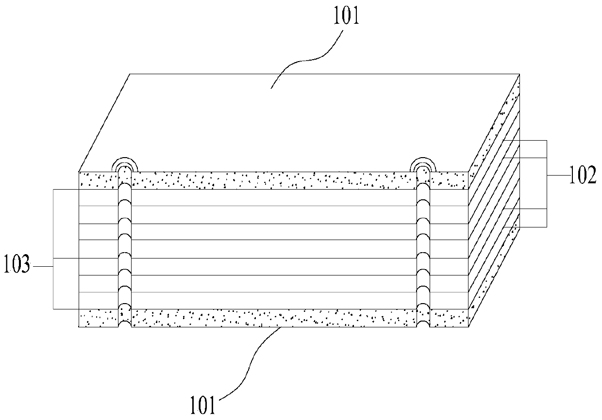
[0036] A high-frequency and high-speed PCB according to the present invention includes at least two layers of rigid base material core boards, at least one layer of PTFE base material core boards and at least one layer of FR4 base material core boards, according to the rigid base material core boards from bottom to top , PTFE base material core board, FR4 base material core board, PTFE base material core board, and rigid base material core board are stacked in sequence, and PTFE type prepregs are pressed between each core board; the main body of the PCB board There are through holes penetrating through the rigid substrate core board, PTFE base material core board and FR4 base material core board.

[0037] The rigid base material core plate adopted in the present invention is a rigid low-loss base material core plate; in a further solution, the low-loss rigid base material of the present invention is a rigid material with slightly worse electrical properties than PTFE, that is, ...


PUM


Abstract

The invention discloses a high-frequency and high-speed printed circuit board (PCB) and a fabrication method thereof. The high-frequency and high-speed PCB comprises at least two layers of rigid substrate core plates, at least one layer of PTFE substrate core plate and at least one layer of FR4 substrate core plate, wherein a PCB main body is formed by sequentially laminating the rigid substrate core plate, the PTFE substrate core plate, the FR4 substrate core plate, the PTFE substrate core plate and the rigid substrate core plate from bottom to top, PTFE prepregs are laminated among the core plates, and a through hole is drilled in the PCB main body. The fabrication method of the high-frequency and high-speed PCB comprises the steps of board cutting, surface roughness processing, inner-layer pattern fabrication, baking plate processing, board lamination, drilling, copper plating, soldering and surface processing. The PCB disclosed by the invention has the characteristics of excellent high-speed / high-frequency transmission and low transmission loss, the production processes such as drilling, shaping and board grinding are easier to control, and the problem that a soldering layer is easy to drop off is solved.

Description

technical field [0001] The invention relates to the technical field of design and manufacture of a printed circuit board (PCB), in particular to a high-frequency and high-speed PCB and a manufacturing method thereof. Background technique [0002] Printed circuit board (PCB) is the carrier of electronic components and electrical connections, and it is widely used in various electronic products. At present, in the process of PCB production, FR4 material is mostly used as the base material for the production of circuit boards, and then the production of circuits is completed on the base material. Due to the limitation of the dielectric constant Dk and dielectric loss factor Df of the FR4 material itself, this substrate is only suitable for printed circuit boards with a transmission rate below 1Gbps. However, with the rapid development of the electronics and communication industries, electronic information products continue to The direction of high frequency and high speed is d...

Claims


Application Information

Patent Timeline
Patent Type & Authority Patents(China)
IPC IPC(8): H05K1/03
Inventor 程柳军王红飞陈蓓
Owner GUANGZHOU FASTPRINT CIRCUIT TECH
Why Eureka
Try Eureka