Electro-optical modulator using ribbed waveguides

A silicon waveguide, conductive type technology, applied in the field of light modulation, can solve the problem of reducing the effectiveness of electro-optical devices

Active Publication Date: 2016-11-16
CISCO TECH INC
View PDF7 Cites 6 Cited by
  • Summary
  • Abstract
  • Description
  • Claims
  • Application Information

AI Technical Summary

Problems solved by technology

High current densities may heat the structure causing undesired thermo-optic effects, and indeed cause an effect opposite to that associated with the movement of free carriers on the actual refractive index change, reducing the effective efficiency of the electro-optic device. sex

Method used


Image

  • Electro-optical modulator using ribbed waveguides
  • Electro-optical modulator using ribbed waveguides
  • Electro-optical modulator using ribbed waveguides

Examples


Embodiment Construction

[0020] overview

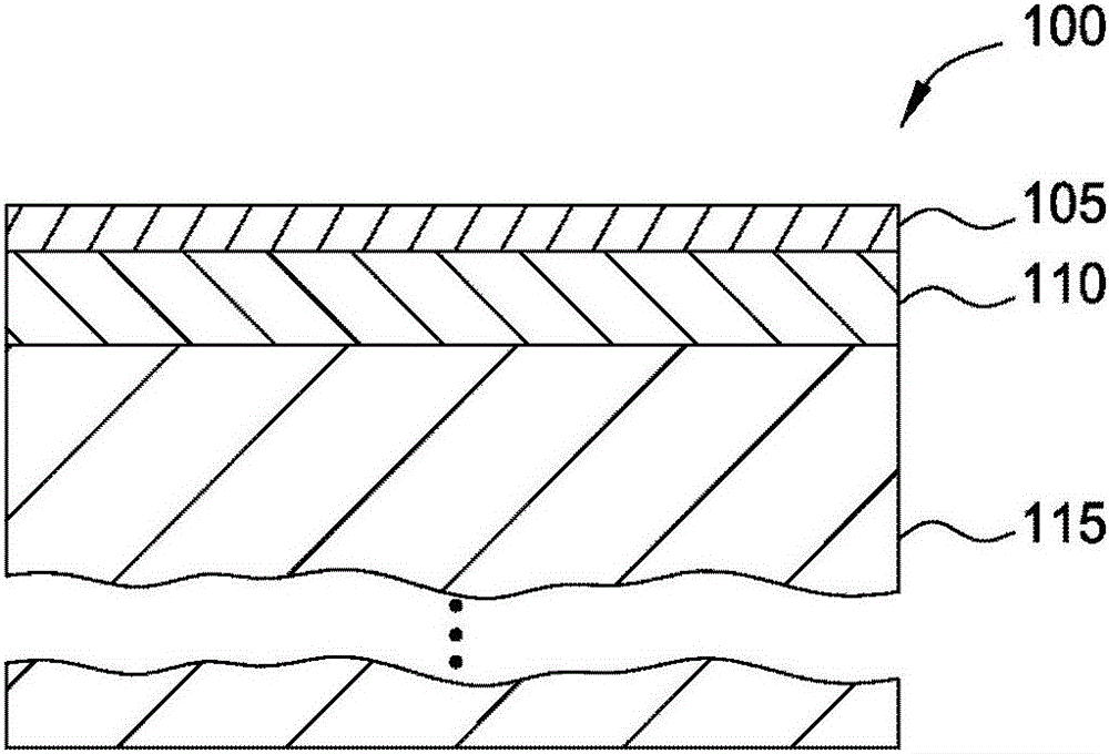
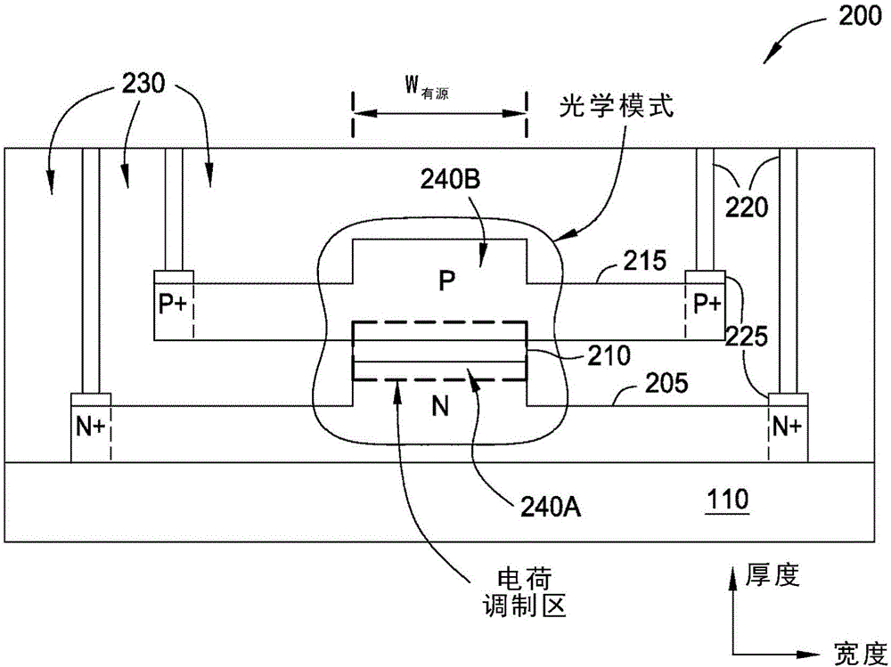
[0021] One embodiment presented by the present disclosure is an optical device comprising a first silicon waveguide disposed on a dielectric base layer, wherein the first silicon waveguide comprises a first ridge extending in the direction of the optical path. The optical device includes a dielectric layer having a lower surface disposed on the upper surface of the first ridge; and a second silicon waveguide disposed on the dielectric layer opposite to the lower surface of the dielectric layer. on the upper surface. The second silicon waveguide includes a second ridge extending in the direction of the light path and overlapping both the dielectric layer and the first ridge. Furthermore, the first silicon waveguide is doped with a first conductivity type and the second silicon waveguide is doped with a second different conductivity type. The optical device also includes a first electrical contact coupled to the first silicon waveguide and a second electric...


PUM

PropertyMeasurementUnit
thicknessaaaaaaaaaa
thicknessaaaaaaaaaa
thicknessaaaaaaaaaa

Abstract

The invention discloses an electro-optical modulator using ribbed waveguides. An optical modulator may include a lower waveguide, an upper waveguide, and a dielectric layer disposed therebetween. When a voltage potential is created between the lower and upper waveguides, these layers form a silicon-insulator-silicon capacitor (also referred to as SISCAP) guide that provides efficient, high-speed optical modulation of an optical signal passing through the modulator. In one embodiment, at least one of the waveguides includes a respective ridge portion aligned at a charge modulation region which may aid in confining the optical mode laterally (e.g., in the width direction) in the optical modulator. In another embodiment, ridge portions may be formed on both the lower and the upper waveguides. These ridge portions may be aligned in a vertical direction (e.g., a thickness direction) so that ridges overlap which may further improve optical efficiency by centering an optical mode in the charge modulation region.

Description

technical field [0001] Embodiments presented in this disclosure relate generally to light modulation, and more specifically, to silicon-based electro-optic modulators. Background technique [0002] Many electro-optic devices exploit the free-carrier dispersion effect to change the real and imaginary parts of the refractive index. This is because unstrained pure crystalline silicon does not exhibit a linear electro-optic (Pockels) effect, and the change in refractive index due to the Franz-Keldish and Kerr effects is very weak. Phase modulation in specific regions of optical devices (e.g., Mach-Zehnder modulators, total internal reflection (TIR)-based structures, crossbars, Y-switches, ring resonators, and Fabry-Perot resonators) Can be used to modulate the output intensity. [0003] The free carrier concentration in electro-optic devices can be varied by carrier injection, accumulation, depletion or inversion. Most of such devices studied to date exhibit some common featu...

Claims


Application Information

Patent Timeline
Patent Type & Authority Applications(China)
IPC IPC(8): G02F1/025
CPCG02F1/011G02F1/025G02F1/2257Y10S977/834G02F1/0152G02B6/132G02B6/136
Inventor 唐纳德·亚当斯普拉卡什·约托斯卡威普库马·帕特尔马克·韦伯斯特
Owner CISCO TECH INC
Why Eureka
Try Eureka