High-speed silicon-based electro-optic modulator

An electro-optical device, silicon-based technology, used in instruments, optics, light guides, etc., can solve problems such as impact and negative light propagation, and achieve the effects of reduced power consumption, low series resistance, and reduced series resistance.

Active Publication Date: 2006-04-26
CISCO TECH INC
View PDF0 Cites 36 Cited by
  • Summary
  • Abstract
  • Description
  • Claims
  • Application Information

AI Technical Summary

Problems solved by technology

Switching speed can be increased by introducing impurities in silicon that act as carrier lifetime "killers", but the introduced impurities have a negative impact on light propagation

Method used


Image

  • High-speed silicon-based electro-optic modulator
  • High-speed silicon-based electro-optic modulator
  • High-speed silicon-based electro-optic modulator

Examples


Embodiment Construction

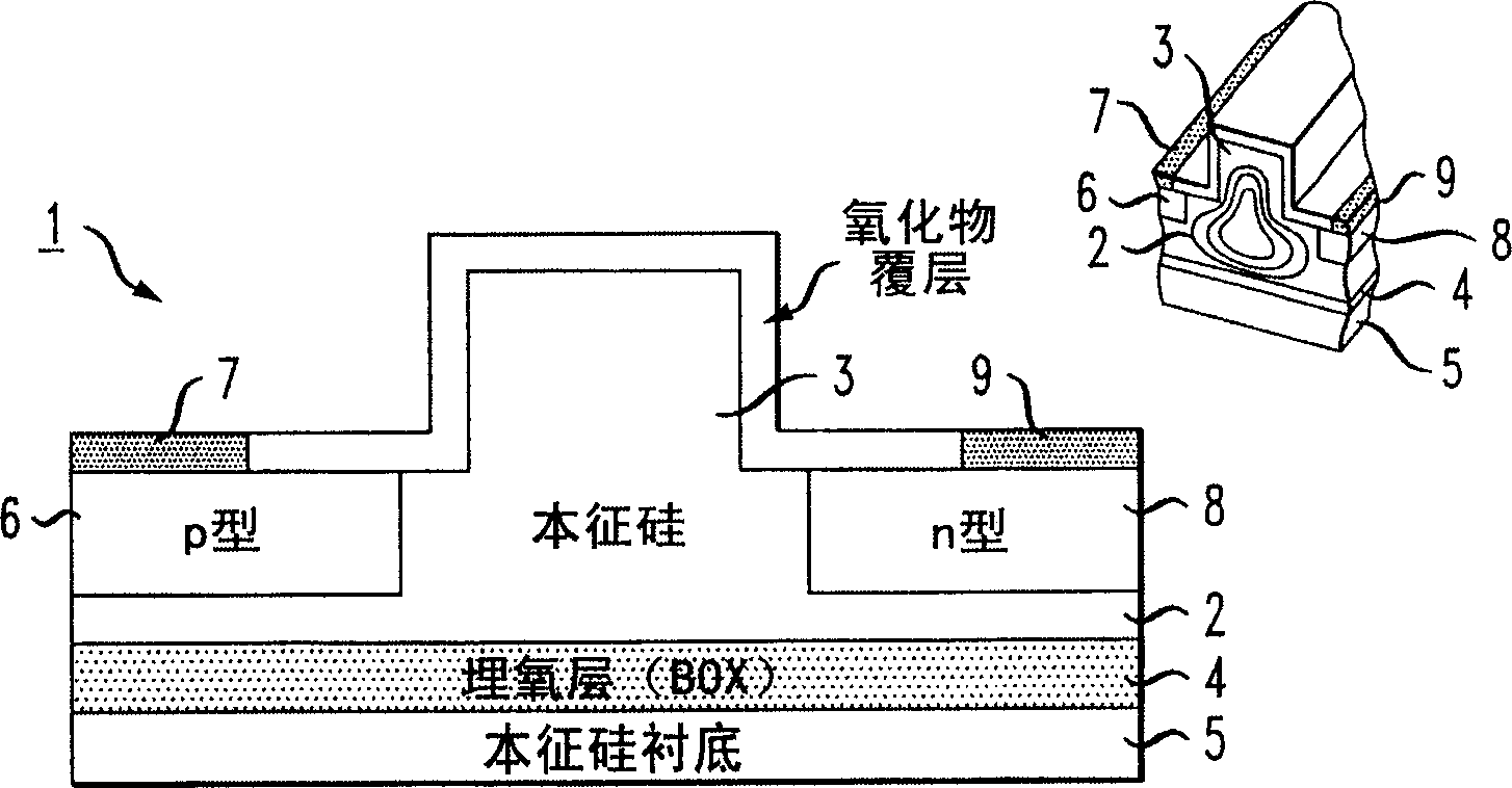
[0046] Before describing the specific typical structure of the silicon-based electro-optic device of the present invention, the following discussion sets out the modulation mechanisms in silicon upon which the present invention operates. It should be understood that although the various embodiments illustrated relate to modulator structures, the SISCAP-based geometry of the present invention can be used with any silicon-based device that utilizes the electro-optical effect (carrier movement) described below.

[0047] As mentioned above, since pure electro-optic effects do not exist or are very weak in silicon, only free carrier dispersion and thermo-optic effects provide potential mechanisms for modulation. For the speeds of current interest (Gb / s and above), only the free carrier dispersion is valid, while the configuration of the present invention is based on the free carrier dispersion by the following correlation relation of the classical Drude model according to the first ...


PUM

PropertyMeasurementUnit
thicknessaaaaaaaaaa
thicknessaaaaaaaaaa
thicknessaaaaaaaaaa

Abstract

A silicon-based electro-optical modulator (30) based on a gate region of the first conductivity formed to partially cover the body region of the second conductivity type, having interposed between the contact portions of the gate region and the body region (12, 10) A relatively thin dielectric layer (10). The modulator may be formed on an SOI platform with a body region formed in a relatively thin silicon surface layer of the SOI structure and a gate region formed with a relatively thin silicon layer (10) overlying the SOI structure. The doping of the control gate and body regions is used to form lightly doped regions above and below the dielectric layer, thereby defining the active region of the device (16). Advantageously, the photoelectric field in the active device region is substantially identical to the free carrier concentration region. Therefore, the application of the modulation signal causes the free carriers on both sides of the dielectric layer to accumulate, deplete or invert simultaneously, resulting in high-speed operation.

Description

[0001] Cross References to Related Applications [0002] This application claims priority to Provisional Application No. 60 / 457,242, filed March 25,2003. technical field [0003] The present invention relates to a silicon-based electro-optic modulator, in particular to an electro-optic modulator based on SOI technology and using a silicon-insulator-silicon capacitor (SISCAP) waveguide geometry to provide high efficiency and high speed operation. Background technique [0004] Due to the possibility of integrating optical components together with advanced electronics on silicon substrates by using well-known CMOS technology, fiber optics operating at 1330 and 1550 nm are used in various systems such as fiber-to-the-home and local area networks (LANs). Silicon-based photonic components at communication wavelengths are the subject of intensive research. [0005] Passive silicon structures such as waveguides, couplers and filters have been extensively studied. In contrast, less...

Claims


Application Information

Patent Timeline
Patent Type & Authority Applications(China)
IPC IPC(8): G02F1/025G02B6/12G02B6/26G02F1/225
CPCG02B2006/12142G02B2006/12159G02F1/025G02F1/2257G02B6/12
Inventor 罗伯特·凯斯·蒙特哥莫里马格利特·吉龙普拉卡什·约托斯卡威普库马·帕特尔卡尔潘都·夏斯特里索哈姆·帕塔克凯瑟琳·A·亚努舍弗斯奇
Owner CISCO TECH INC
Why Eureka
Try Eureka