Semiconductor device

A semiconductor and chip technology, applied in semiconductor devices, semiconductor/solid-state device components, output power conversion devices, etc., to solve problems such as noise, malfunction, and noise transmission

Inactive Publication Date: 2016-11-16
DENSO CORP
View PDF6 Cites 6 Cited by
  • Summary
  • Abstract
  • Description
  • Claims
  • Application Information

AI Technical Summary

Problems solved by technology

[0008] In such a structure, if a short circuit occurs and a large current flows momentarily between the main terminal arranged in line with the control terminal and another main terminal, noise will be generated due to the magnetic coupling between the main terminal arranged in line with the signal path, and there is a risk of Possible noise transmission in the signal path and malfunction

Method used


Image

  • Semiconductor device
  • Semiconductor device
  • Semiconductor device

Examples


no. 1 Embodiment approach

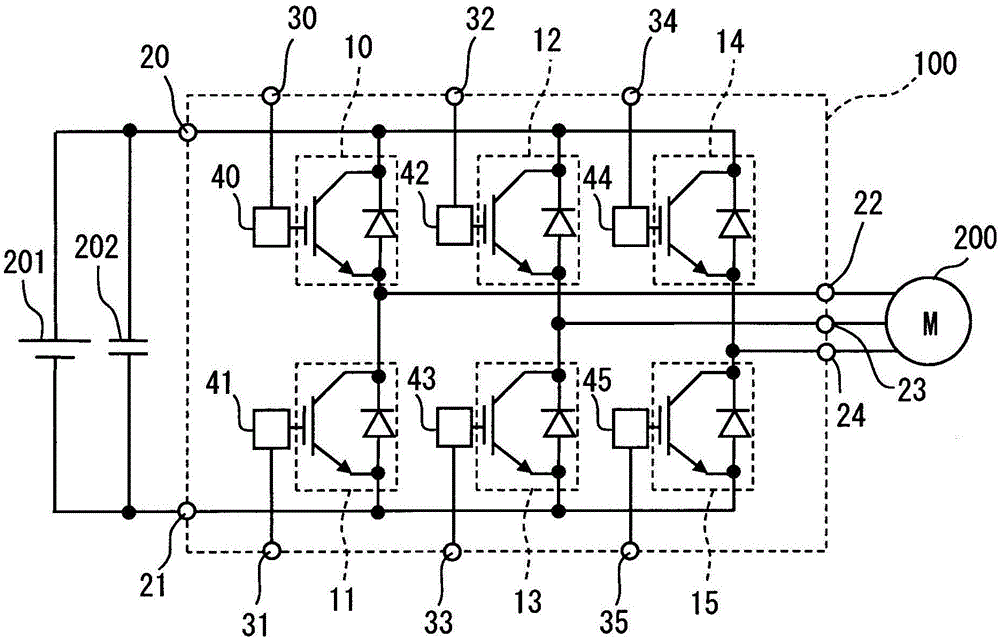
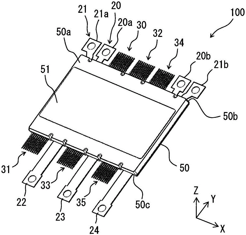
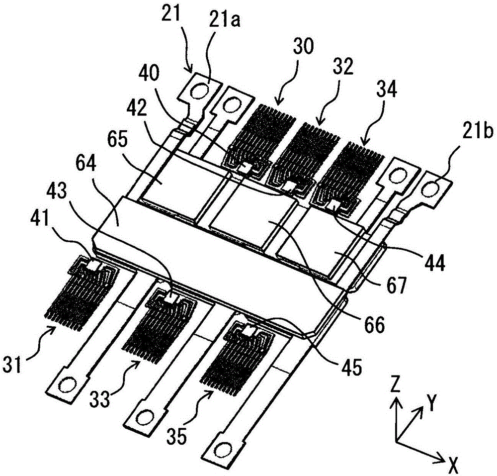
[0041] First, based on Figure 1 to Figure 6 The configuration of the semiconductor device 100 according to this embodiment will be described.

[0042] Such as figure 1 As shown, the semiconductor device 100 has three-phase upper and lower arms connected between the positive pole (high potential side) and the negative pole (low potential side) of the DC power supply 201 in order to drive the motor 200 as a load. In this way, the semiconductor device 100 is configured as a three-phase converter, which converts DC power into a three-phase AC and outputs it to the motor 200 . Such a semiconductor device 100 is mounted in, for example, an electric vehicle or a hybrid vehicle. in addition, figure 1 Reference numeral 202 is shown as a capacitor for smoothing.

[0043]A semiconductor chip constituting each arm has a power switching element such as an IGBT or a MOSFET, and a FWD element connected in antiparallel to the switching element. In addition, the power switching element...

no. 2 Embodiment approach

[0090] In this embodiment, descriptions of parts common to the semiconductor device 100 described in the first embodiment are omitted.

[0091] The technical concept of making the combined inductances of the five signal paths substantially equal to make the noise voltages generated in the respective signal paths substantially equal when the large current 75 flows instantaneously is the same as that of the first embodiment.

[0092] In this embodiment, if Figure 15 and Figure 16 As shown, output terminals 22 to 24 are provided in pairs, respectively. The U-phase output terminal 22 is branched and has two output terminals 22a and 22b. Furthermore, in the X direction, they are arranged on both sides of the signal path of the U-phase lower arm so as to sandwich the U-phase control terminal 31 , that is, the signal path including the control terminal 31 . Similarly, the V-phase output terminal 23 is branched to have two output terminals 23a and 23b. Then, in the X direction, ...


PUM


Abstract

A semiconductor device (100), in which a plurality of control terminals (31) that correspond to a main terminal (22) and the same semiconductor chip (11) protrude from a surface (50c) of a sealing part (50), and a plurality of signal paths that include the plurality of control terminals are positioned so as to be aligned with the main terminal in a first direction. Provided in each of the plurality of signal paths are pairs of relay members having identical functions, and a first relay grouping (71) that includes one relay member of the pair of relay members and a second relay grouping (72) that includes the other relay member of the pair are positioned neighboring each other aligned in the first direction, with the ordering of the first relay grouping being mirror-inverted relative to the second relay grouping.

Description

[0001] Cross-references to related applications [0002] This disclosure claims priority based on Japanese Patent Application No. 2014-64195 filed on March 26, 2014, the entire content of which is incorporated herein. technical field [0003] The present disclosure relates to semiconductor devices. Background technique [0004] Conventionally, a plurality of control terminals serving as main terminals and corresponding to the same semiconductor chip protrude from one surface of the sealing part, signal paths including the control terminals are arranged in a row in the first direction, and the main terminals are connected to the signal path in the first direction. A structure described in Patent Document 1 is known as a semiconductor device arranged side by side in a path. [0005] The semiconductor device described in Patent Document 1 has six semiconductor elements (semiconductor chips) for constituting a three-phase converter. A wiring member (main terminal) is connected...

Claims


Application Information

Patent Timeline
Patent Type & Authority Applications(China)
IPC IPC(8): H01L25/07H01L23/50H01L25/18
CPCH01L23/49537H01L23/49541H01L23/49562H01L23/49568H01L23/49575H01L25/07H01L25/18H01L2224/48137H01L2224/49171H01L2224/49175H01L2924/13055H01L2924/13091H01L23/50H01L2924/00H01L23/3121H02M7/003H02M7/537H02P27/06
Inventor 岩渕明金森淳小野田宪司大前翔一朗
Owner DENSO CORP
Why Eureka
Try Eureka