Wafer encapsulation method

A chip packaging and chip technology, applied in the manufacture of electrical components, electrical solid devices, semiconductor/solid devices, etc., can solve the problems of time-consuming and high cost, reduce reflow baking, improve bonding ability, and hinder thermal diffusion Effect

Inactive Publication Date: 2016-11-23
双峰发展顾问有限公司
View PDF4 Cites 0 Cited by
  • Summary
  • Abstract
  • Description
  • Claims
  • Application Information

AI Technical Summary

Problems solved by technology

[0002] like figure 1 and figure 2 As shown, the existing packaging method of the chip 1 is to adopt the reflow (FC) package body to use the flux 2 on the substrate 4, and the solder ball 5 is arranged under the substrate 4. During the packaging process, there are three processes of reflow baking and flux cleaning. But the disadvantage is high cost, labor and time-consuming

Method used


Image

  • Wafer encapsulation method
  • Wafer encapsulation method
  • Wafer encapsulation method

Examples


Embodiment Construction

[0022] In order to further explain the technical solution of the present invention, the present invention will be described in detail below through specific examples.

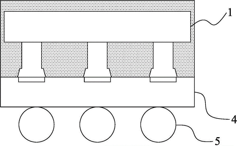
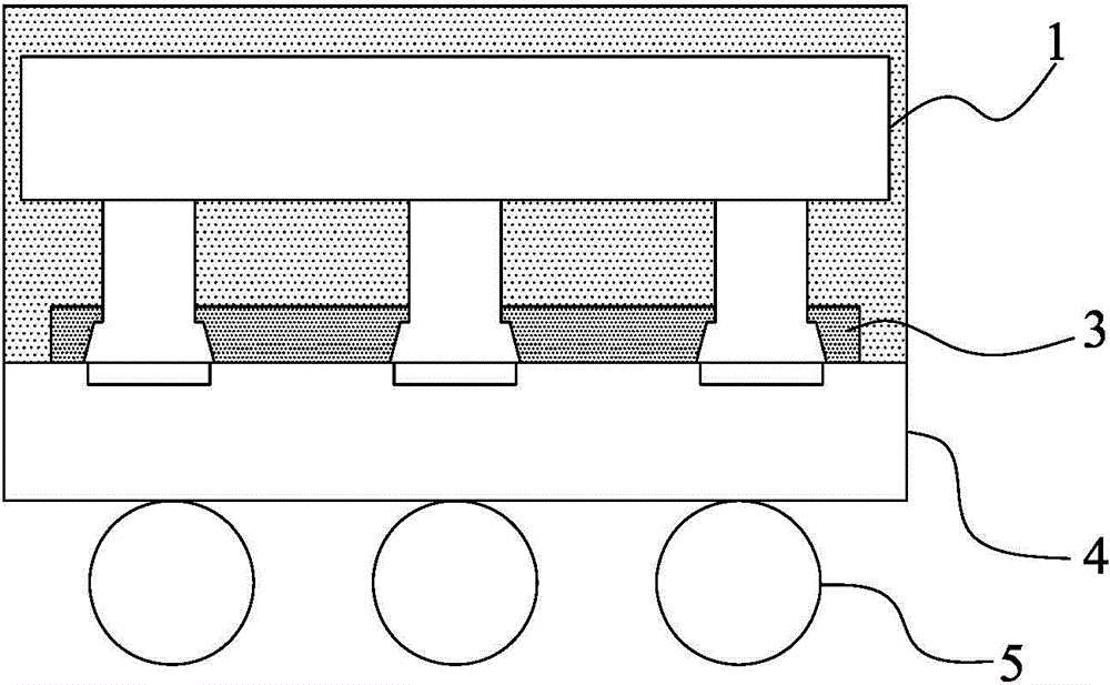
[0023] Such as image 3 The structure containing non-conductive glue (NCP) of the present invention is to apply flux 2 on the copper pillar between the integrated circuit 1 and the substrate 4, and connect the two by welding, and the substrate 4 is coated with non-conductive glue (NCP) 3. Solder balls 5 are arranged under the substrate to form a packaged integrated circuit structure.

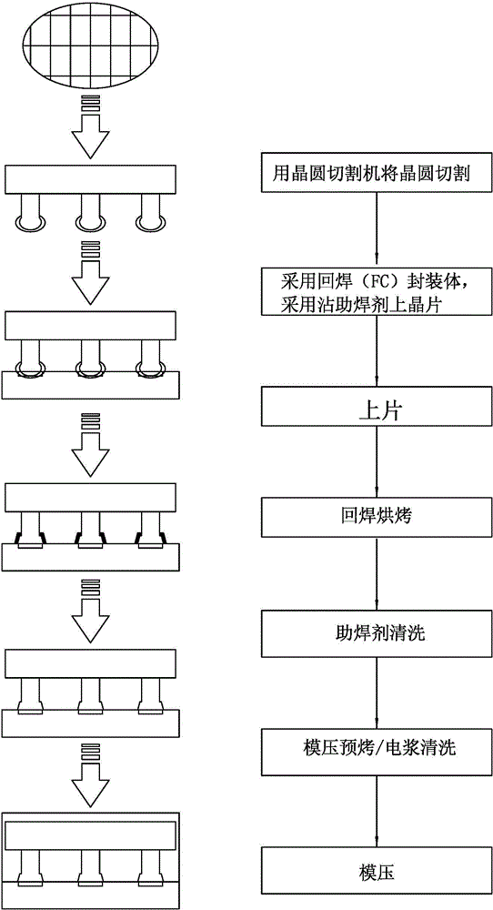
[0024] Such as Figure 4 Shown, a kind of chip packaging method of the present invention comprises the following steps:

[0025] The wafer is cut by a wafer cutting machine, and then the wafer is picked up by the loading equipment, and the tin bumps of the wafer are stained with flux.

[0026] Then use the glue material printing equipment to apply the non-conductive glue (NCP) on the front of the substrate by steel plate print...


PUM


Abstract

The invention discloses a wafer encapsulation method. The method comprises the following steps that: a wafer cutter is utilized to cut a wafer, a wafer is sucked by a wafer mounting device, and the tin bumps of the wafer are coated with soldering flux; a paste coating and printing device is utilized to apply non-conductive paste onto the front surface of a substrate by means of steel plate printing, rubber head transfer or air valve jet printing; the tin bumps are directly welded on the copper pads of the substrate through using a post-tin melting welding technology under 290 DEG C to 300 DEG C; a post-wafer mounting material is baked, and plasma cleaning and resin mould pressing encapsulation are carried out; and a post-tin melting welding encapsulation body can be obtained. According to the wafer encapsulation method of the invention, the post-tin melting welding encapsulation body is obtained through a post-tin melting welding procedure; the post-tin melting welding encapsulation body requires the application of one non-conductive paste layer onto the surface of the substrate, and a paste coating and printing machine has a built-in non-conductive paste coating function, and therefore, work hours are not affected. Compared with a conventional wafer encapsulation process, the wafer encapsulation method does not contain reflow baking and soldering flux washing, and therefore, equipment can be reduced, and manpower and soldering flux cleaning costs can be also decreased.

Description

technical field [0001] The invention relates to a chip packaging method. Background technique [0002] Such as figure 1 and figure 2 As shown, the existing packaging method of the chip 1 is to adopt the reflow (FC) package body to use the flux 2 on the substrate 4, and the solder ball 5 is arranged under the substrate 4. During the packaging process, there are three processes of reflow baking and flux cleaning. But the disadvantage is high cost and time-consuming. [0003] The reflow (FC) package is only suitable for wide pitch (Wide Pitch) bumps chip packaging, not suitable for fine pitch (Fine Pitch) bumps chip packaging (after the tin bumps dipped in flux are baked in a reflow oven, the tin will Flux thermal diffusion, fine gap ((Fine Pitch), Cu trace to Cu trace<60um distance between copper wire and copper wire is less than 60um). Contents of the invention [0004] The purpose of the present invention is to provide a chip packaging method that can reduce the pa...

Claims


Application Information

Patent Timeline
IPC IPC(8): H01L21/60
CPCH01L24/81H01L2224/81355H01L2224/81H01L2924/181H01L2924/00012
Inventor 刘正仁
Owner 双峰发展顾问有限公司
Why Eureka
Try Eureka