Supercharge Your Innovation With Domain-Expert AI Agents!

Boost circuit for improving transient response

A transient response and circuit technology, applied in the electronic field, can solve problems such as slow transient response of BOOST circuit, large overshoot and drop of output voltage, and poor transient response, so as to improve transient response and reduce output voltage drop , to ensure the stability of the system

Active Publication Date: 2016-11-23
SPREADTRUM COMM (SHANGHAI) CO LTD
View PDF4 Cites 7 Cited by
  • Summary
  • Abstract
  • Description
  • Claims
  • Application Information

AI Technical Summary

Problems solved by technology

[0002] BOOST circuits are widely used in mobile devices such as smart phones and tablet computers due to their characteristics of low power supply voltage, low power consumption, high efficiency, high output voltage and large output current. According to different control mechanisms, BOOST circuits are divided into PWM (Pulse Width Modulation) control mode, PFM (PulseFrequency Modulation) control mode and hybrid control mode. The hybrid control mode adopts the PWM working mode under the heavy load condition, and switches to the PFM working mode under the light load condition to ensure the whole load The converters in the range have high conversion efficiency. However, the transient response of the existing BOOST circuit is slow, which seriously affects the performance of the chip. At the same time, there is a large overshoot and drop in the output voltage when the load jumps. Refer to figure 1 circuit diagram and figure 2 It can be seen from the waveform diagram that figure 2 From top to bottom in the figure are the waveform diagrams of load current Iload, output voltage Vout, and junction node Lx. When the load current suddenly increases, the transient response is poor, which affects the normal function realization of the system.

Method used


Image

  • Boost circuit for improving transient response
  • Boost circuit for improving transient response
  • Boost circuit for improving transient response

Examples


specific Embodiment

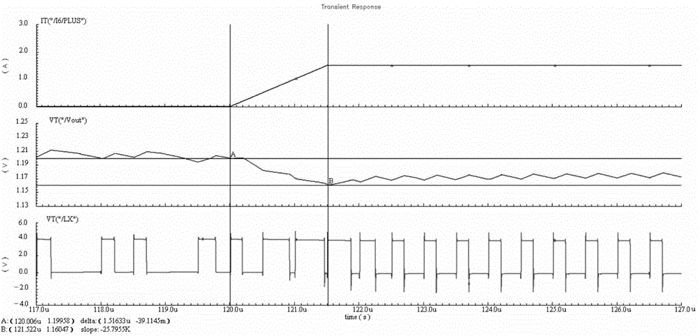
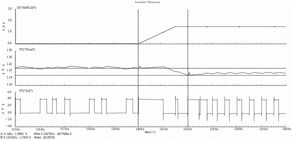
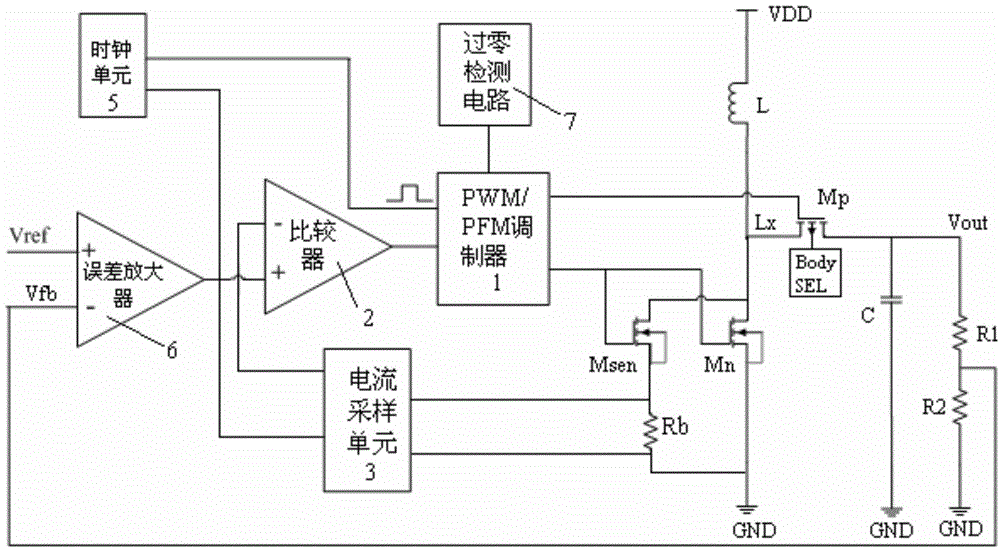
[0057] A specific embodiment, an N-channel MOS transistor Mn is connected in series on the charge control branch, a P-channel MOS transistor Mp is connected in series on the discharge control branch, the substrate of the N-channel MOS transistor Mn is connected to a control signal Body SEL, a load The capacitor C is connected between the output terminal Vout and the ground terminal GND, and the resistance R1 and the resistance R2 connected in series are also connected between the output terminal Vout and the ground terminal GND. The points connected between the voltage dividing resistors form a voltage dividing node, and the voltage feedback signal It is drawn from the point where resistor R1 and resistor R2 are connected.

[0058] In the BOOST circuit for improving transient response of the present invention, the current detection signal is generated by a current detection circuit, and the current detection circuit may include,

[0059] A detection resistor Rb, connected in s...


PUM


Abstract

The invention relates to the technical field of electronics, and particularly relates to a BOOST circuit for improving the transient response. The circuit comprises a working circuit provided with an energy storage element, a switching device assembly and a control unit. The working circuit is used for generating an output voltage higher than an input voltage. The switching device assembly is used for controlling the working circuit to be alternately switched between the charging mode and the discharging mode under the effect of a PWM modulation signal or a PFM modulation signal. The control unit is used for generating the PWM modulation signal or the PFM modulation signal according to a reference voltage, a voltage feedback signal sampled from the output end of the switching voltage regulator, a current detection signal sampled from the working circuit and a switching control signal, and then generating a modulating signal of a preset duty ratio within a preset time period. According to the technical scheme of the invention, when a load is increased transiently, a predetermined duty cycle is generated, such as a modulation signal with a duty ratio of 99%. Therefore, the capacitor of the load is fully charged, and the reduction of the output voltage is lowered. The transient response of the circuit can be improved and the system stability is ensured.

Description

technical field [0001] The invention relates to the field of electronic technology, in particular to a BOOST circuit. Background technique [0002] BOOST circuits are widely used in mobile devices such as smart phones and tablet computers due to their characteristics of low power supply voltage, low power consumption, high efficiency, high output voltage and large output current. According to different control mechanisms, BOOST circuits are divided into PWM (Pulse Width Modulation) control mode, PFM (PulseFrequency Modulation) control mode and hybrid control mode. The hybrid control mode adopts the PWM working mode under the heavy load condition, and switches to the PFM working mode under the light load condition to ensure the whole load The converters in the range have high conversion efficiency. However, the transient response of the existing BOOST circuit is slow, which seriously affects the performance of the chip. At the same time, there is a large overshoot and drop in...

Claims


Application Information

Patent Timeline
Patent Type & Authority Applications(China)
IPC IPC(8): H02M3/07
Inventor 樊茂刘程斌
Owner SPREADTRUM COMM (SHANGHAI) CO LTD
Features
  • R&D
  • Intellectual Property
  • Life Sciences
  • Materials
  • Tech Scout
  • Unparalleled Data Quality
  • Higher Quality Content
  • 60% Fewer Hallucinations
Learn More