High-frequency SAW (Surface Acoustic Wave) device based on Si substrate and manufacturing method thereof

A high-frequency and device technology, applied in the field of Si-based high-frequency SAW devices and their preparation, can solve the problems of low Si phase velocity and affect the center frequency of multi-layer structure SAW devices, and achieve high electromechanical coupling coefficient and small volume. Effect

Inactive Publication Date: 2016-11-23
UNIV OF ELECTRONICS SCI & TECH OF CHINA
View PDF7 Cites 7 Cited by
  • Summary
  • Abstract
  • Description
  • Claims
  • Application Information

AI Technical Summary

Problems solved by technology

[0004] In order to be compatible with the integrated circuit process, most of the diamond or diamond-like films are deposited on Si substrates, but the thickness of diamond or diamond-like films is on the order of nanometers, so that part of the excited surface acoustic waves propagates in Si, while The phase velocity of Si is small, which affects the center frequency of the multilayer structure SAW device

Method used


Image

  • High-frequency SAW (Surface Acoustic Wave) device based on Si substrate and manufacturing method thereof
  • High-frequency SAW (Surface Acoustic Wave) device based on Si substrate and manufacturing method thereof

Examples


Embodiment Construction

[0022] In order to enable a clear and complete description of the technical solution of the present invention, further description will be given with reference to the accompanying drawings.

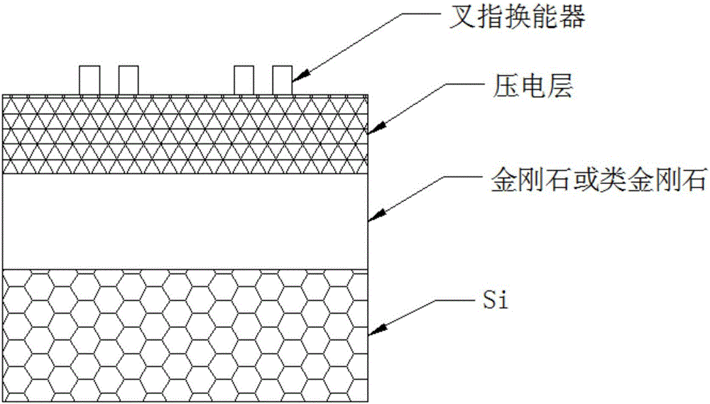
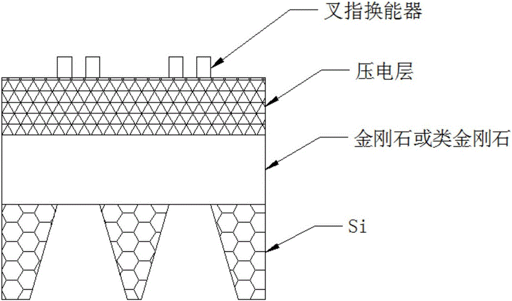
[0023] prepared as figure 2 A Si-based high-frequency SAW device is shown.

[0024] Step 1. Using CVD to grow a diamond film with a thickness of 500nm on a Si substrate with a thickness of 2mm, polishing it with CMP to make the roughness 10nm, and then cleaning to obtain a diamond / Si substrate.

[0025] Step 2, using radio frequency magnetron sputtering to deposit a layer of AlN film with a thickness of 200nm on the diamond / Si substrate.

[0026] Step 3. Spin-coat a layer of photoresist on both sides of AlN / diamond / Si with a glue spinner, and make a pattern on the back of Si by photolithography, and soak in 10% KOH for 5 minutes, and make a pattern on the back of Si. Such as figure 2 The number of grooves shown is 2, the side of the trapezoidal cross-section is 0.6mm, the length of t...


PUM

PropertyMeasurementUnit
Thicknessaaaaaaaaaa
Roughnessaaaaaaaaaa
Thicknessaaaaaaaaaa

Abstract

The invention relates to the field of manufacturing of SAW (Surface Acoustic Wave) devices, in particular to a high-frequency SAW device based on a Si substrate and a manufacturing method thereof. The high-frequency SAW device has a multilayer membrane structure, and comprises the Si substrate, a high-acoustic-speed layer, a piezoelectric layer and interdigital transducers in sequence from bottom to top. A back side of the Si substrate is provided with slots, so that transmission of surface acoustic waves is limited in the high-acoustic-speed layer in order to increase the center frequency of the device. The SAW device with the multi-membrane structure can satisfy high-frequency and high electromechanical coupling coefficients and meet the application demands in the field of integrated circuits. Compared with a piezoelectric single-crystal material, a piezoelectric membrane adopted in the piezoelectric layer is easy to integrate, and can be applied to the semiconductor industry.

Description

technical field [0001] The invention relates to the field of SAW device manufacturing, in particular to a Si-based high-frequency SAW device and a preparation method thereof. Background technique [0002] With the rapid development of mobile communication technology, the frequency of use of surface acoustic wave (SAW) devices has been increasing, from the initial MHz level to the current GHz level. The frequency of the SAW device is proportional to the sound wave propagation velocity of the material, and inversely proportional to the period of the interdigital transducer (IDT). Therefore, increasing the frequency of the SAW device can be done from two aspects. One is to make the fingers of the IDT thinner. The second is to adopt materials with higher SAW propagation speed. The method of thinning the IDT fingers is simple and direct, but the thinning of the fingers will also cause some disadvantages. For example, the thinning of the IDT fingers to the sub-micron level will b...

Claims


Application Information

Patent Timeline
IPC IPC(8): H03H9/02H03H3/04
CPCH03H9/02661H03H3/04H03H2003/023H03H2003/0414
Inventor 帅垚李杰吴传贵罗文博陈留根蒲诗睿潘忻强白晓圆
Owner UNIV OF ELECTRONICS SCI & TECH OF CHINA
Why Eureka
Try Eureka