Magneto-optic material gap waveguide magnetic surface fast wave direction-controllable photodiode
A magneto-optical material and photodiode technology, applied in optics, nonlinear optics, instruments, etc., can solve the problems of polarization angle loss, inapplicability of Faraday isolators, complex structure, etc., and achieve easy integration, simple structure, and small volume Effect
- Summary
- Abstract
- Description
- Claims
- Application Information
AI Technical Summary
Problems solved by technology
Method used
Image
Examples
Embodiment 1
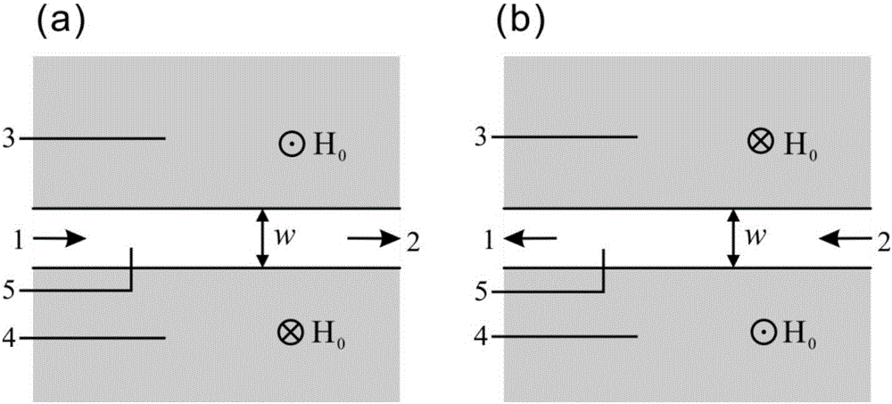
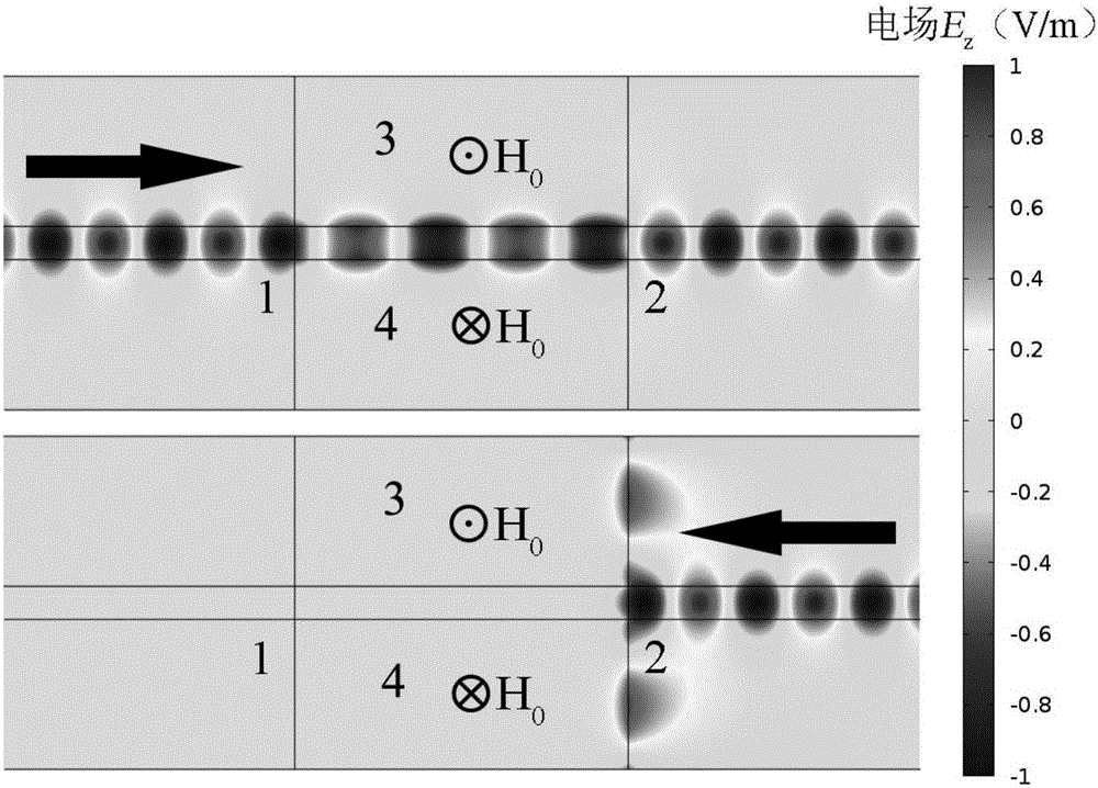
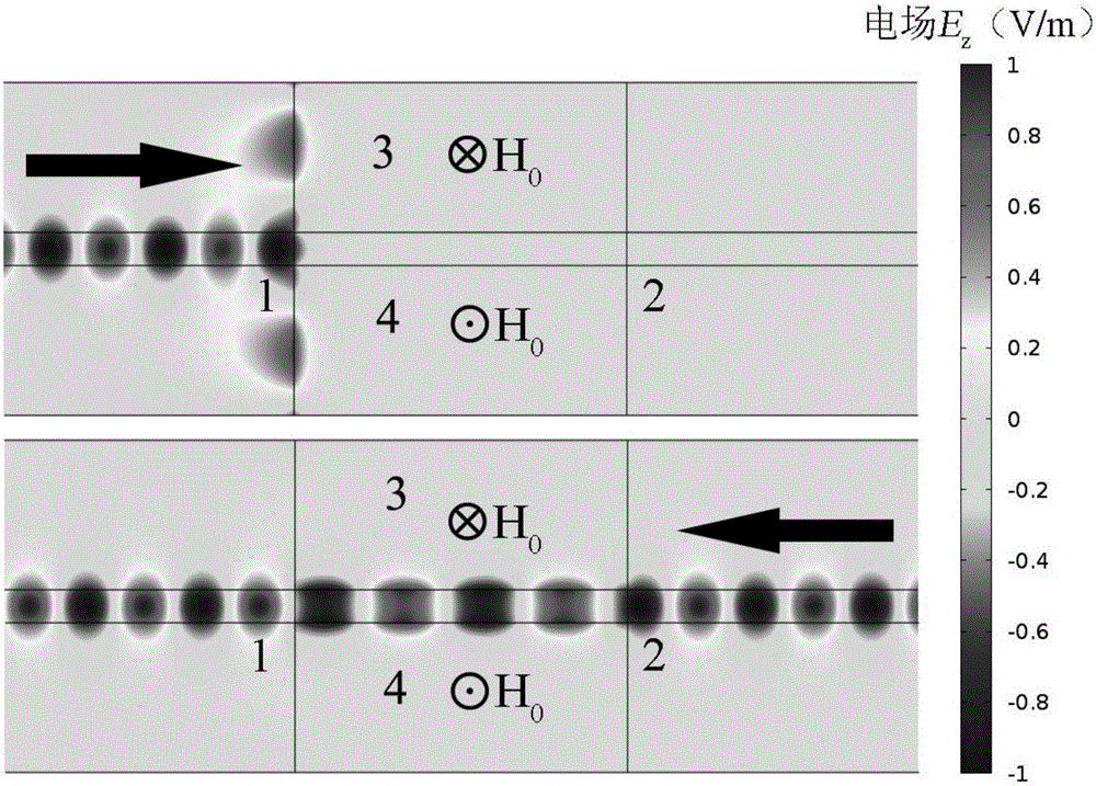
[0044] refer to figure 1 (a) and (b), the magnetic surface fast wave direction controllable photodiode is composed of a magneto-optical material gap waveguide, and the dielectric layer 5 is air (n 0 =1), its thickness w=5mm. In the working frequency band, control the direction of the magnetic field at 3 places perpendicular to the paper surface outward through the electromagnet current, and the direction of the magnetic field at 4 places perpendicular to the paper surface inward, and the photodiode will conduct from port ” to port 2; on the contrary, control the direction of the magnetic field at 3 places vertically The paper faces inward, the direction of the magnetic field at 4 places is perpendicular to the paper, and the photodiode will conduct from port 2 to port 1. The forward and reverse transmission efficiency of these two cases is the same. Refer to Figure 4 , The operating frequency range of the photodiode and the isolator with the straight waveguide structure is 5...
Embodiment 2
[0046] refer to figure 1 (a) and (b), the magnetic surface fast wave direction controllable photodiode is composed of a magneto-optical material gap waveguide, and the dielectric layer 5 is air (n 0 =1), its thickness w=7mm. In the working frequency band, the direction of the magnetic field at the first magneto-optical material layer 3 is controlled outwardly by the direction of the paper, and the direction of the magnetic field at the second layer of magneto-optic material 4 is inward, and the photodiode will pass from port 1 to the port 2 conduction; on the contrary, control the direction of the magnetic field at the first magneto-optical material layer 3 to the inside of the paper, and the direction of the magnetic field at the second magneto-optic material layer 4 to the outside of the paper, and the photodiode will conduct from port 2 to port 1 . The forward and reverse transmission efficiencies of the two cases are the same. refer to Figure 5 , The operating frequen...
Embodiment 3
[0048] refer to figure 1 (a) and (b), the magnetic surface fast wave direction controllable photodiode is composed of a magneto-optical material gap waveguide, and the dielectric layer 5 is glass (n 0 =1.5), its thickness w=5mm. In the working frequency band, the direction of the magnetic field at the first magneto-optical material layer 3 is controlled outwardly by the direction of the paper, and the direction of the magnetic field at the second layer of magneto-optic material 4 is inward, and the photodiode will pass from port 1 to the port 2 conduction; on the contrary, control the direction of the magnetic field at the first magneto-optical material layer 3 to be perpendicular to the plane of the paper, and the direction of the magnetic field at the second magneto-optical material layer 4 to be perpendicular to the plane of the paper to be outward, and the photodiode will be conducted from port 2 to port 1. The forward and reverse transmission efficiencies of the two case...
PUM
| Property | Measurement | Unit |
|---|---|---|
| Thickness | aaaaa | aaaaa |
Abstract
Description
Claims
Application Information


