Optical fingerprint sensor module

A fingerprint sensor, optical technology, applied in the acquisition/organization of fingerprints/palmprints, instruments, characters and pattern recognition, etc., can solve problems such as performance needs to be improved, and achieve the effect of improving performance

Inactive Publication Date: 2016-12-07
SHANGHAI OXI TECH
View PDF5 Cites 53 Cited by
  • Summary
  • Abstract
  • Description
  • Claims
  • Application Information

AI Technical Summary

Problems solved by technology

[0005] The structure of the existing optical fingerprint sensor mo

Method used


Image

  • Optical fingerprint sensor module
  • Optical fingerprint sensor module
  • Optical fingerprint sensor module

Examples


Embodiment Construction

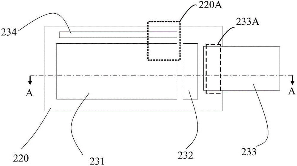
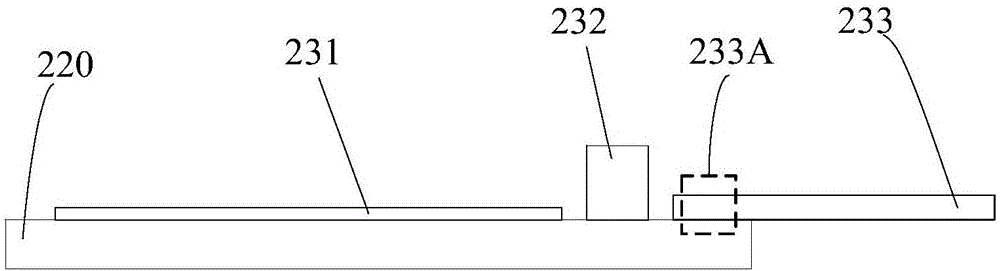
[0036] In an existing optical fingerprint sensor, such as figure 2 and image 3 The structure shown, where figure 2 is the top view of the optical fingerprint sensor, image 3 for figure 2 Optical fingerprint sensor shown along figure 2The cross-sectional schematic diagram obtained by cutting A-A dot-dash line. The optical fingerprint sensor includes a glass substrate 220 , and a pixel array area 231 and peripheral circuits on the glass substrate 220 . The peripheral circuit area includes a driving circuit 234 , a signal readout chip 232 and a flexible printed circuit board 233 . The pixel array area 231 includes a pixel array for receiving, converting and temporarily storing optical signals. Described peripheral circuit area also comprises flexible printed circuit board binding area 233A, the connection line between the binding area of ​​pixel array area 231, signal readout chip 232 and the binding area of ​​flexible printed circuit board 233 (each connection line i...


PUM

PropertyMeasurementUnit
Thicknessaaaaaaaaaa
Thicknessaaaaaaaaaa

Abstract

The invention discloses an optical fingerprint sensor module. The optical fingerprint sensor module comprises an optical fingerprint sensor, a protective layer, a backlight source and a touching sensing layer, wherein the optical fingerprint sensor comprises a light-transmitting substrate and a device layer located on the surface of the light-transmitting substrate, the device layer comprises a pixel area, the pixel area has a plurality of pixels, all the pixels comprise light-transmitting areas and non-light-transmitting areas, the non-light-transmitting areas comprise photosensitive elements, and the light-transmitting areas allow a light ray to be capable of penetrating through the pixel area of the device layer; the protective layer is located above the optical fingerprint sensor; the backlight source is located below the optical fingerprint sensor, and an included angle formed between a light ray emitted by the backlight source and the surface of the pixel area is an acute angle; the touching sensing layer is located between the protective layer and the optical fingerprint sensor. According to the optical fingerprint sensor module, the structure and the performance are improved, and the function is enhanced.

Description

technical field [0001] The invention relates to the field of optical fingerprint identification, in particular to an optical fingerprint sensor module. Background technique [0002] Fingerprint imaging recognition technology is to collect the fingerprint image of the human body through the optical fingerprint sensor, and then compare it with the existing fingerprint imaging information in the system to judge whether it is correct or not, and then realize the technology of identity recognition. Due to its ease of use and the uniqueness of human fingerprints, fingerprint imaging recognition technology has been widely used in various fields. For example, security inspection areas such as public security bureaus and customs, building access control systems, and consumer products such as personal computers and mobile phones, etc. The realization of fingerprint imaging recognition technology includes optical imaging, capacitive imaging, ultrasonic imaging and other technologies. ...

Claims


Application Information

Patent Timeline
IPC IPC(8): G06K9/00
CPCG06V40/1324G06V40/1306G06F3/0421G06F2203/04103G06V40/1329G06V40/1318
Inventor 凌严朱虹
Owner SHANGHAI OXI TECH
Why Eureka
Try Eureka