Silicon-based microdisplay module group

A micro-display, silicon-based technology, applied to static indicators, instruments, etc., can solve the problems that silicon-based micro-display modules have not yet appeared, and achieve the effect of high display refresh rate, high display resolution, and improved transmission rate

Inactive Publication Date: 2016-12-07
LUMICORE MICROELECTRONICS SHANGHAI CO LTD
View PDF7 Cites 14 Cited by
  • Summary
  • Abstract
  • Description
  • Claims
  • Application Information

AI Technical Summary

Problems solved by technology

At present, the existing silicon-based microdisplay technology has a resolution of 800*600 and adopts a digital in

Method used


Image

  • Silicon-based microdisplay module group
  • Silicon-based microdisplay module group
  • Silicon-based microdisplay module group

Examples


Embodiment 1

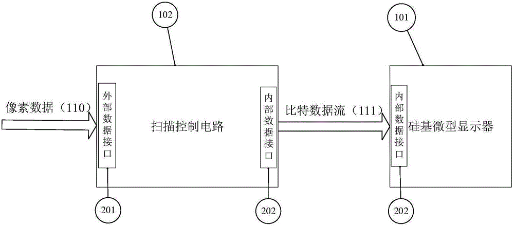
[0044] see figure 1 , the silicon-based micro-display module is characterized in that the silicon-based micro-display and the scanning control circuit are connected through a differential interface, and all light-emitting devices of the silicon-based micro-display are manufactured on the same single-crystal silicon chip through semiconductor technology, and all transistors formed by it are All work in digital switch mode, with only two states of "on" and "off", using digital pulse width modulation to control the brightness and grayscale of pixels. The scanning control circuit receives externally input pixel data and sends the bit plane data to the silicon-based microdisplay through a differential interface.

Embodiment 2

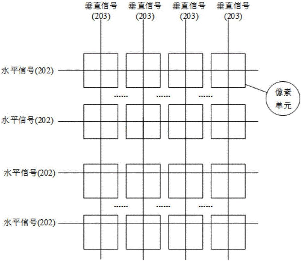
[0046] see figure 2 , The silicon-based microdisplay is characterized in that the visible area of ​​the silicon-based microdisplay is any one of rectangle, square, rhombus, ellipse and perfect circle. The pixel array is arranged in matrix form, and the bright and dark states of the pixels are controlled by horizontal signals and vertical signals. A metal sheet is pasted under the silicon-based microdisplay for heat dissipation. The material of the metal sheet can be Al, Cu, Ag, Au, Pt, Cr, W, Mo, Ti, TiN, Sn, ITO, ZnO or these materials compound between.

Embodiment 3

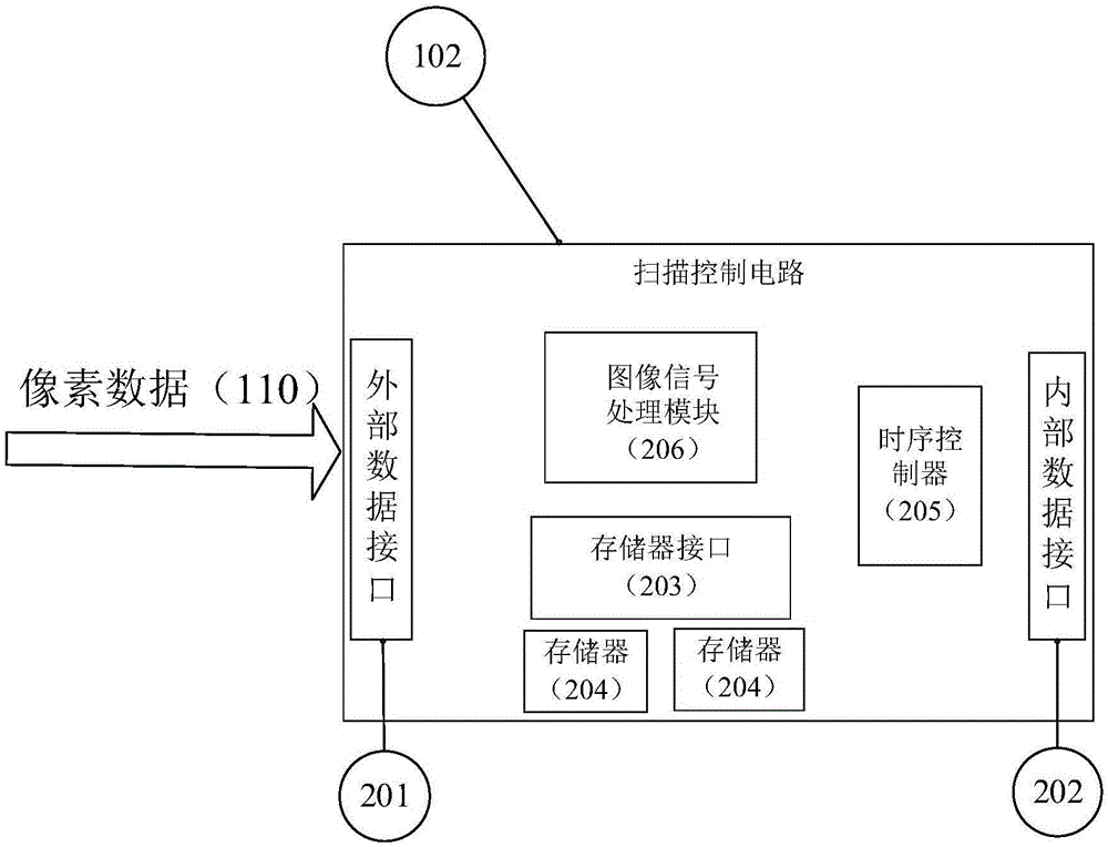
[0048] see image 3 , the scanning control circuit is characterized in that the scanning control circuit includes an external data interface, a memory interface, a memory, a timing controller, an image signal processing module, and an internal data interface for receiving pixel data, and the external data interface receives external external input Pixel data, its types include but not limited to VGA, A / V, DVI, HDMI, RGB, YCbCr, LVDS, MIPI, DisplayPort, eDP, PCI-Express, USB, IEEE1394. The memory is a dynamic memory or a static memory for storing pixel data. The timing controller is used to generate bit-plane timing signals to refresh silicon-based microdisplays. The image signal processing module reads the pixel data of the memory and performs image scaling, image rotation, gamma correction, YUV conversion to RGB, image enhancement, edge enhancement, grayscale nonlinear correction, image distortion correction and other processing. The internal data interface is a differentia...


PUM


Abstract

The invention discloses a silicon-based microdisplay module group. The module group comprises a silicon-based microdisplay (101) and a scanning control circuit (102). The silicon-based microdisplay (101) is made on a monocrystalline silicon substrate. Each pixel only has bright and dark states. Through a digital pulse width, a gray scale of the pixel is modulated. The scanning control circuit (102) receives external input pixel data (110) through an external data interface (201) and outputs a bit data flow (111) through an internal data interface (202) according to a sequence of bit planes. The module group integrates luminescent devices on a monocrystalline silicon chip. A total number of system chips can be reduced so as to decrease system cost and power consumption. A product size is reduced and a wide application prospect is possessed. The module group can be applied to fields of head-mounted display, a portable computer, virtual reality display, medical electronics, military electronics and the like.

Description

technical field [0001] The invention relates to the field of semiconductor displays, in particular to a silicon-based microdisplay module. Background technique [0002] The silicon-based microdisplay module includes two basic components, a silicon-based microdisplay and a scanning control circuit. Silicon-based microdisplay is a kind of microdisplay that uses semiconductor technology to directly manufacture light-emitting pixels on the surface of single crystal silicon. Each pixel of this silicon-based microdisplay has only two states: bright and dark. Grayscale, and all pixels on the silicon-based microdisplay are arranged in a matrix, and the light and dark states of the pixels are controlled by horizontal and vertical signals; the scanning control circuit converts the externally input pixel data into bit-plane data and outputs it to the silicon-based On the microdisplay, the silicon-based microdisplay is connected with the silicon-based microdisplay control circuit throu...

Claims


Application Information

Patent Timeline
IPC IPC(8): G09G3/20
CPCG09G3/2014G09G3/2096G09G2310/0267
Inventor 季渊刘万林冉峰
Owner LUMICORE MICROELECTRONICS SHANGHAI CO LTD
Why Eureka
Try Eureka