Manufacturing method of flash memory embedded into logic circuit

A manufacturing method and a technology of logic circuit area, applied in the direction of circuit, semiconductor/solid-state device manufacturing, electrical components, etc., can solve the problems of pinhole effect, easy short circuit of logic transistor, low yield rate of flash memory, etc. The effect of a large process window

Active Publication Date: 2016-12-07
SEMICON MFG INT (SHANGHAI) CORP
View PDF3 Cites 3 Cited by
  • Summary
  • Abstract
  • Description
  • Claims
  • Application Information

AI Technical Summary

Problems solved by technology

[0005] In recent years, with the development of flash memory, in order to improve storage reliability and extend storage life, flash memory is required to have a thicker tunnel insulating layer and a floating gate. To match this, the gate oxide layer of the high-voltage transistor It also needs to be thicker, and the logic transistor of the logic circuit needs a thinner gate oxi

Method used


Image

  • Manufacturing method of flash memory embedded into logic circuit
  • Manufacturing method of flash memory embedded into logic circuit
  • Manufacturing method of flash memory embedded into logic circuit

Examples


Embodiment Construction

[0036] As mentioned in the background, in the prior art, when a flash memory, a high-voltage floating-gate transistor, and a logic transistor are manufactured simultaneously, the channel of the logic transistor may have a pinhole effect, and adjacent logic transistors may be easily short-circuited. In view of the above technical problems, the inventors have found the following three reasons after analysis.

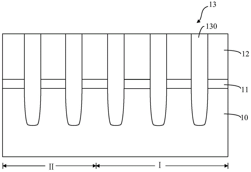
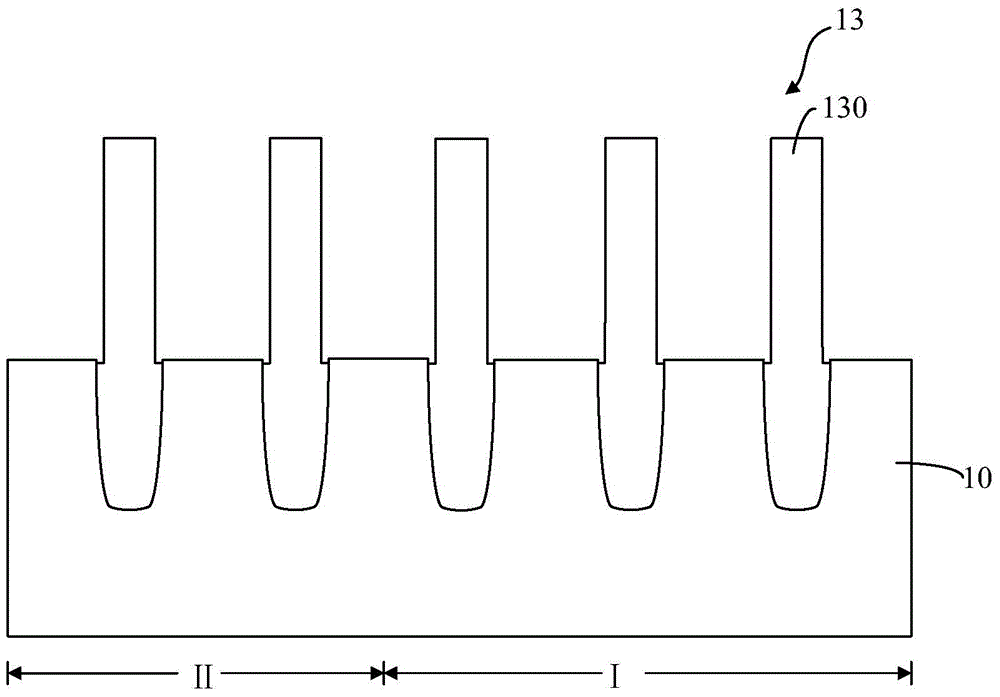
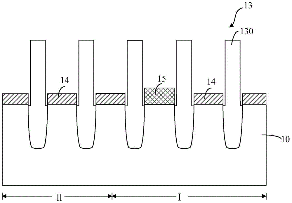
[0037] 1) Reference Figure 1 to Figure 3 As shown, in order to form the tunnel insulating layer required for the flash memory and the high-voltage floating gate transistor in the core cell area I, the buffer oxide layer 11 and the silicon nitride layer 12 stacked on the surface of the semiconductor substrate 10 from bottom to top After the shallow trench isolation structure 13 is formed, the silicon nitride layer 12 in the core cell region I and the logic circuit region II is removed first, and then the buffer oxide layer 11 is removed. The buffer oxide layer 11 is made ...


PUM


Abstract

The invention provides a manufacturing method of a flash memory embedded into a logic circuit. When a gate oxide layer of a logic transistor and tunneling insulating layers of the flash memory and a high-voltage floating gate transistor are formed, a buffer oxide layer with relatively low density is removed, so that insulating materials, corroded by an HF acid, in shallow trench isolation structures are relatively few; gaps between the insulating materials and the semiconductor substrate are relatively small; the residual conductive polycrystalline silicon is also relatively little; the adjacent flash memory, high-voltage floating gate transistor and logic transistor extending along the shallow trench isolation structures are not easy to short-circuit; and a process window is relatively large. Furthermore, removal of silicon nitride on the buffer oxide layer is divided into the following two steps of firstly carrying out dry etching on one part of thickness and then removing the remaining thickness through a wet process. The damage to a channel of the logic transistor and the channel of the flash memory or the high-voltage floating gate transistor at the lower part of the buffer oxide layer is avoided.

Description

technical field [0001] The invention relates to the technical field of semiconductors, in particular to a manufacturing method of a flash memory embedded in a logic circuit. Background technique [0002] Random access memory, such as DRAM and SRAM, has the problem of data loss after power failure during use. To overcome this problem, various nonvolatile memories have been designed and developed. Recently, flash memory based on floating gate concept has become the most general non-volatile memory due to its small cell size and good performance. [0003] A structure commonly used in flash memory is a stack gate structure. The stacked gate structure memory includes a tunnel insulating layer, a floating gate polysilicon layer (ploy 1) for storing electrons, and an oxide / nitride-oxide (ONO) layer formed sequentially on the substrate. Stack and control gate polysilicon layer (ploy 2) for electron storage and release. [0004] To complete the writing, erasing and reading of the...

Claims


Application Information

Patent Timeline
IPC IPC(8): H01L21/8247
Inventor 王新鹏
Owner SEMICON MFG INT (SHANGHAI) CORP
Why Eureka
Try Eureka