Array substrate, preparation method of array substrate and display device

A technology for array substrates and substrates, applied in semiconductor/solid-state device manufacturing, instruments, semiconductor devices, etc., can solve the problems of small grain size, low crystal quality, and limited electrical performance of thin-film transistor devices

Active Publication Date: 2016-12-07
BOE TECH GRP CO LTD
View PDF5 Cites 35 Cited by
  • Summary
  • Abstract
  • Description
  • Claims
  • Application Information

AI Technical Summary

Problems solved by technology

[0005] However, due to the existence of the metal light-shielding layer, the heat dissipation rate of the source region and the drain region is very slow compared with that of the channel region. When excimer laser annealing converts amorphous silicon into polysilicon, the channel regi

Method used


Image

  • Array substrate, preparation method of array substrate and display device
  • Array substrate, preparation method of array substrate and display device
  • Array substrate, preparation method of array substrate and display device

Examples


Example Embodiment

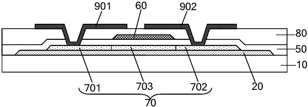
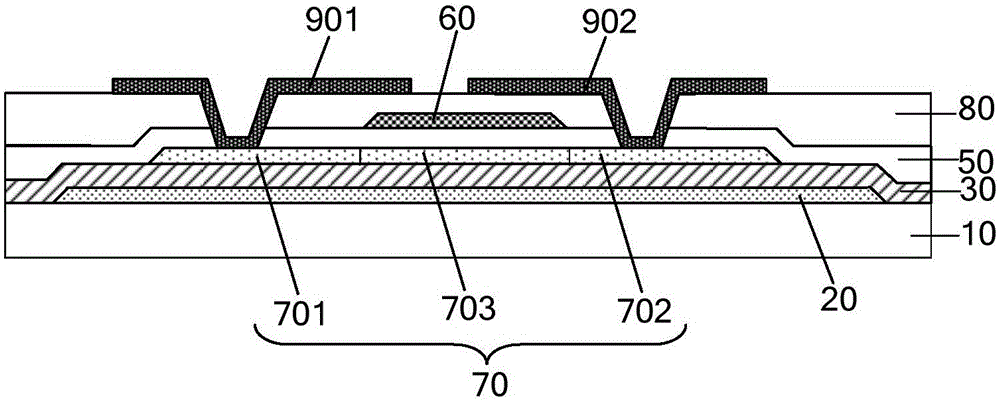
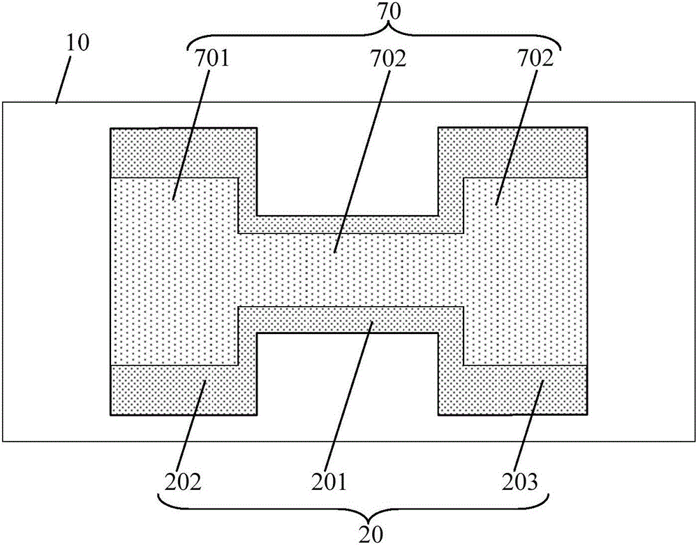
[0083] The embodiment of the present invention also provides a method for preparing the array substrate, such as figure 1 with figure 2 As shown, including forming a polysilicon thin film transistor on a substrate 10, the polysilicon thin film transistor includes an active layer 70, the active layer 70 includes a source region 701, a drain region 702, located in the source region 701 and the drain region 702 Between the channel region 703; wherein the active layer 70 is obtained by ion implantation of the polysilicon layer; the polysilicon layer 402 is obtained by performing excimer laser annealing on the amorphous silicon layer; the method further includes: forming the polysilicon layer Before thin film transistors, a metal light-shielding layer 20 corresponding to the active layer 70 is formed on the substrate 10; the orthographic projection of the metal light-shielding layer 20 on the substrate 10 completely covers the orthographic projection of the channel region 703 on the ...


PUM

PropertyMeasurementUnit
Thermal conductivityaaaaaaaaaa
Thicknessaaaaaaaaaa

Abstract

The embodiment of the invention provides an array substrate, a preparation method of the array substrate and a display device and relates to the technical field of display. The grain size and homogeneity can be improved. The array substrate comprises a substrate and a polycrystalline silicon thin film transistor arranged on the substrate. The polycrystalline silicon thin film transistor comprises an active layer. The active layer comprises a source electrode region, a drain electrode region and a channel region located between the source electrode region and the drain electrode region. The array substrate further comprises a metal light shading layer arranged between the substrate and the active layer. The orthographic projection of the channel region on the substrate is completely covered with the orthographic projection of the metal light shading layer on the substrate, and the metal light shading layer at least covers partial of the source electrode region and partial of the drain electrode region. The method is used for preparing the array substrate.

Description

technical field [0001] The present invention relates to the field of display technology, in particular to an array substrate, a preparation method thereof, and a display device. Background technique [0002] Low Temperature Poly-Silicon-Thin Film Transistor (LTPS-TFT for short) displays have the advantages of high resolution, fast response, high brightness, high aperture ratio, and high electron mobility. [0003] At present, a low-temperature polysilicon thin film transistor includes an active layer, a gate insulating layer, a gate electrode, a source electrode, and a drain electrode arranged on a substrate; the active layer includes a source region, a drain region, and a and the channel region between the drain region. In order to avoid leakage current generated by light irradiating the channel region of the active layer and affecting the electrical performance of the polysilicon thin film transistor, a metal light-shielding layer needs to be provided at a position corres...

Claims


Application Information

Patent Timeline
IPC IPC(8): H01L27/12H01L21/77H01L27/32G02F1/1362
CPCG02F1/1362H01L21/77H01L27/1214H01L2021/775H10K59/00H10K59/12G02F1/133385G02F1/1368H01L29/78603H01L29/78675H01L29/78696H01L29/66757H01L27/1218H01L27/1281H01L27/1285G02F1/13685H10K59/126H10K50/87H01L29/78633H01L27/1296H01L27/1262
Inventor 刘政李小龙
Owner BOE TECH GRP CO LTD
Why Eureka
Try Eureka