Fin field effect transistor forming method

A fin field effect and transistor technology, applied in semiconductor devices, electrical components, circuits, etc., can solve problems such as poor transistor performance and reliability, and achieve the effect of improving performance and eliminating blocking ability.

Active Publication Date: 2016-12-07
SEMICON MFG INT (SHANGHAI) CORP
View PDF3 Cites 1 Cited by
  • Summary
  • Abstract
  • Description
  • Claims
  • Application Information

AI Technical Summary

Problems solved by technology

[0005] FinFETs formed with prior art techniques suffer from poo

Method used


Image

  • Fin field effect transistor forming method
  • Fin field effect transistor forming method
  • Fin field effect transistor forming method

Examples


Example Embodiment

[0027] As the feature size of the fin field effect transistor formed in the prior art is further reduced, the performance and reliability of the fin field effect transistor are poor.

[0028] Figure 1 to Figure 7b It is a schematic structural diagram of the formation process of a fin field effect transistor in an embodiment of the present invention.
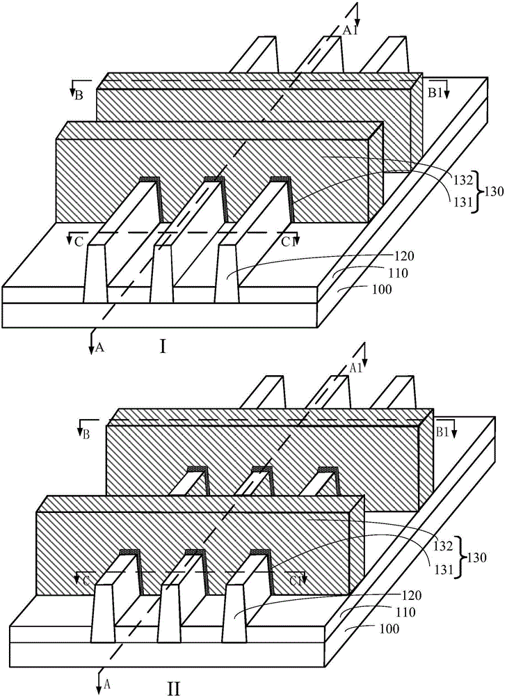
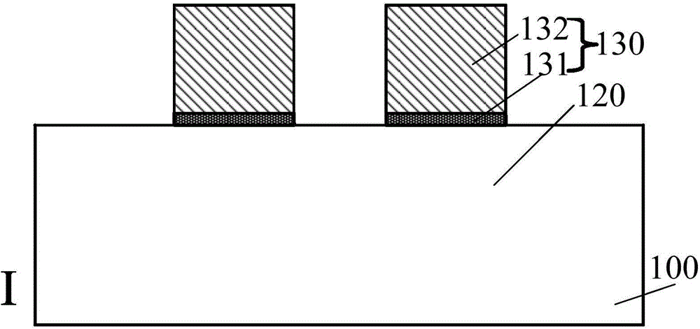
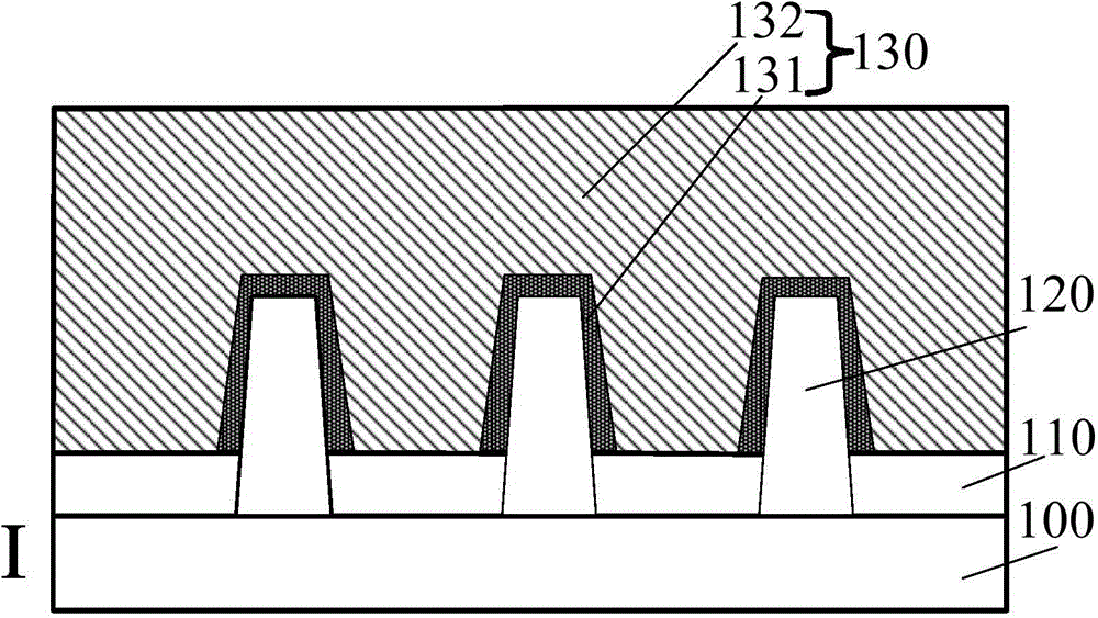
[0029] Combined reference figure 1 , Figure 2a , Figure 2b , Figure 2c , Figure 3a , Figure 3b with Figure 3c , A semiconductor substrate 100 is provided. The semiconductor substrate 100 has a dense gate structure (I area) and a sparse gate structure (II area). The surface of the semiconductor substrate 100 has a raised fin 120 and a cross fin 120, the gate structure 130 covers a part of the top and sidewalls of the fin 120.

[0030] Figure 2a Fin field effect transistor along figure 1 A cross-sectional view of the extension direction of the fin in the middle I region (A-A1 axis), Figure 2b Fin field effect transistor along f...


PUM

PropertyMeasurementUnit
Etching depthaaaaaaaaaa

Abstract

The invention discloses a fin field effect transistor forming method. The method comprises steps: a semiconductor substrate is provided, wherein the semiconductor substrate is provided with a gate structure dense region and a gate structure sparse area, and the surface of the semiconductor substrate is provided with convex fin parts and gate structures crossing the fin parts; a side wall material layer is formed, and the side wall material layer coats the fin parts and the gate structures; first etching is carried out on the side wall material layer, first side walls are formed at two sides of the fin parts in the gate structure dense region, second side walls are formed at two sides of the fin parts in the gate structure sparse region, and the first side walls and the second side walls are lower than the top surfaces of the fin parts; second etching is carried out on fin parts at two sides of the gate structures, first fin parts are formed, the first side walls are flush with the first fin parts, and the second side walls are higher than the first fin parts; third etching is carried out to reduce the height difference between the second side wall and the first fin part; and source and drain areas are formed on the first fin part. The fin field effect transistor forming method of the invention can improve the performance of the fin field effect transistor.

Description

technical field [0001] The invention relates to the field of semiconductor manufacturing, in particular to a method for forming a fin field effect transistor. Background technique [0002] MOS transistors are one of the most important components in modern integrated circuits. The basic structure of a MOS transistor includes: a semiconductor substrate; a gate structure located on the surface of the substrate, and source and drain regions located in the semiconductor substrate on both sides of the gate structure. MOS transistors generate switching signals by applying a voltage to the gate and regulating the current through the channel at the bottom of the gate structure. [0003] With the development of semiconductor technology, the control ability of the channel current of the traditional planar MOS transistor becomes weaker, resulting in serious leakage current. Fin Field Effect Transistor (Fin FET) is an emerging multi-gate device, which generally includes a fin protrudin...

Claims


Application Information

Patent Timeline
IPC IPC(8): H01L29/66H01L21/28
Inventor 韩秋华
Owner SEMICON MFG INT (SHANGHAI) CORP
Why Eureka
Try Eureka