Processing method for ultrathin multi-layer printed circuit board

A technology for printed circuit boards and processing methods, applied in multilayer circuit manufacturing, printed circuits, printed circuit manufacturing, etc., can solve problems such as low efficiency and yield, rising production costs, and complicated operations, and reduce difficulty and risk. , the effect of increasing productivity

Active Publication Date: 2016-12-07
SHANGHAI MEADVILLE SCI & TECH
View PDF8 Cites 7 Cited by
  • Summary
  • Abstract
  • Description
  • Claims
  • Application Information

AI Technical Summary

Problems solved by technology

[0010] The key issue of this method is: the processing of inner core board
However, when the thickness of the dielectric layer of the core plate is less than 50 μm, special and expensive ultra-thin core plate processing equipment must be used for processing, and the production cost will increase significantly
The industry also uses auxiliary tools to proces

Method used


Image

  • Processing method for ultrathin multi-layer printed circuit board
  • Processing method for ultrathin multi-layer printed circuit board
  • Processing method for ultrathin multi-layer printed circuit board

Examples


Embodiment Construction

[0055] The present invention will be further described below in conjunction with the embodiments and accompanying drawings.

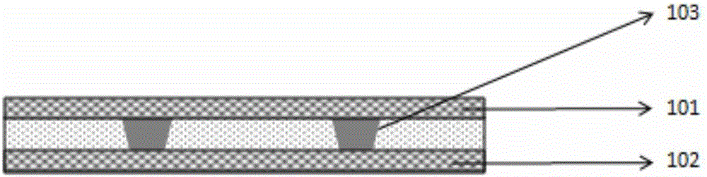
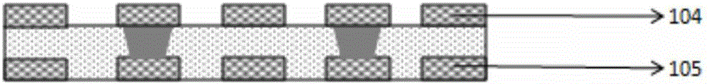
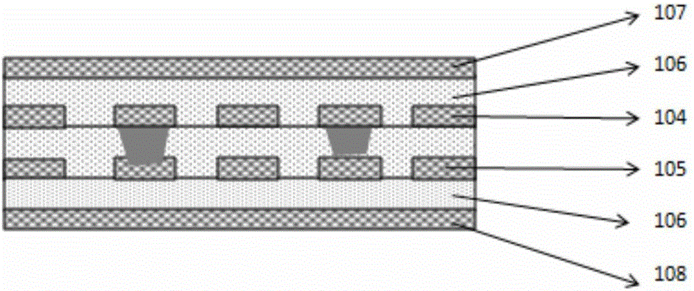
[0056] The main manufacturing process of any interlayer interconnection ultra-thin printed circuit board or semiconductor integrated circuit packaging substrate of the present invention is as follows, taking the ultra-thin six-layer circuit board processing flow as an example:

[0057] The first step is to prepare an ultra-thin carrier copper foil of a specific size. The structure is that an ultra-thin copper foil 202, 202' of 2-5 microns is attached to a carrier copper foil 201, 201' of 12 or 18 microns. In addition, the ultra-thin copper foil 202 and the carrier copper foil 201, the ultra-thin copper foil 202' and the carrier copper foil 201' can be disassembled, and the specific size can be determined according to the actual production situation, which is usually the minimum plate size for the production line process. The ultra-thin carrier copper fo...


PUM

PropertyMeasurementUnit
Thicknessaaaaaaaaaa
Thicknessaaaaaaaaaa
Thicknessaaaaaaaaaa

Abstract

A processing method for an ultrathin multi-layer printed circuit board comprises the following steps of firstly, simultaneously laminating and pressing an ultrathin carrier copper foil and a carrier prepreg to form a detachable multi-layer structure circuit bard having a carrier structure, attaching and fixing the ultrathin copper foil onto the carrier structure by gummosis of carrier prepreg resin to form an unified integral structure, determining an alignment system by a positioning hole in the ultrathin carrier copper foil for subsequent flow process, and separating processing boards from the ultrathin copper foil and the carrier copper foil by edge milling and plate disassembly operation when the thicknesses of the processing boards are larger than or equal to 0.06 millimeters, thereby obtaining two completely same processing circuit boards; and finally, respectively processing the two processing boards by a conventional process flow until the fabrication of a required circuit or package substrate is completed. By the processing method, the cost can be substantially reduced, and the production efficiency and the product yield are improved.

Description

technical field [0001] The present invention relates to a printed circuit board or a semiconductor integrated circuit manufacturing technology, in particular to a processing method for an ultra-thin multilayer printed circuit board, and more particularly to an ultra-thin multilayer printed circuit board or a semiconductor integrated circuit with any layer interconnection The invention discloses a processing method of an ultra-thin multilayer printed circuit board in the process of manufacturing a package substrate. Background technique [0002] As electronic products enter the era of functionalization and intelligence, the development trend of high integration, miniaturization, and miniaturization is becoming more and more urgent. Printed circuit boards or semiconductor integrated circuit packaging substrates are the premise of satisfying the good electrical and thermal performance of electronic products. Under the current situation, it is also developing towards light, thin...

Claims


Application Information

Patent Timeline
IPC IPC(8): H05K3/46
CPCH05K3/4632H05K3/4638H05K2203/068
Inventor 陈明明程分喜常明
Owner SHANGHAI MEADVILLE SCI & TECH
Why Eureka
Try Eureka