Super junction device

A super junction device and gate structure technology, applied in semiconductor devices, electrical components, circuits, etc., can solve the problems of increasing MOSFET loss, many holes, residues, etc., and achieve the effect of reducing the maximum reverse recovery current

Active Publication Date: 2016-12-14
上海鼎阳通半导体科技有限公司
View PDF3 Cites 41 Cited by
  • Summary
  • Abstract
  • Description
  • Claims
  • Application Information

AI Technical Summary

Problems solved by technology

However, in some occasions, when the MOSFET is turned off, there are still more holes remaining, and at this time the MOSFET will undergo reverse recovery.
A large reverse recovery current will increase the loss of the MOSFET, and may also lead to the conduction of the parasitic triode, resulting in damage to the device

Method used


Image

  • Super junction device
  • Super junction device
  • Super junction device

Examples


Embodiment Construction

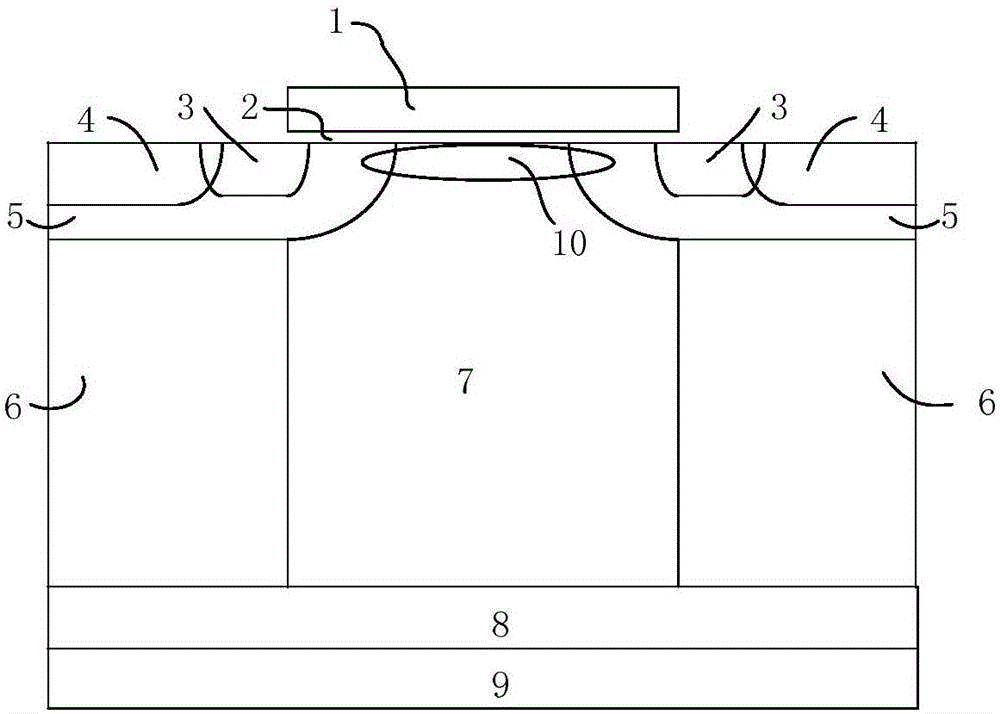
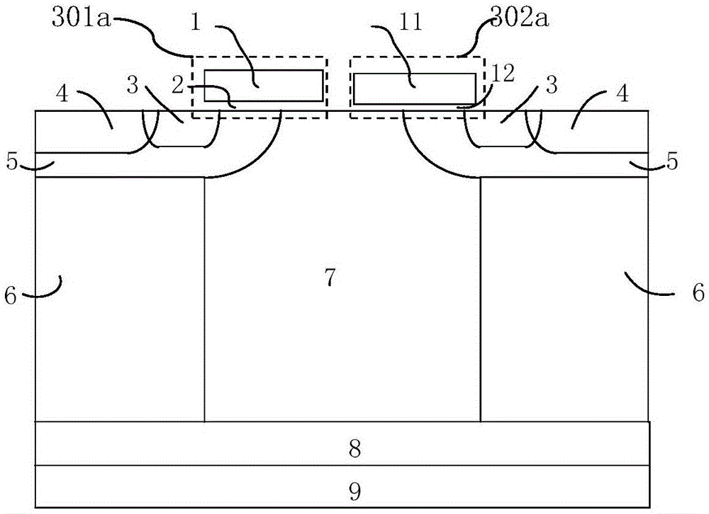
[0057] Such as figure 2 Shown is the structure diagram of the super junction device of the first embodiment of the present invention; the super junction device of the first embodiment of the present invention includes:

[0058] A super junction structure composed of alternately arranged N-type pillars 7 and P-type pillars 6 . The N-type column 7 is directly composed of an N-type epitaxial layer. The P-type column 6 is formed by forming a groove in the N-type epitaxial layer and then filling it with P-type silicon. In other embodiments, the P-type column 6 can also be used multiple times. Epitaxy plus photolithography and ion implantation.

[0059] A P-type doped channel region 5 is formed on the top of each P-type column 6 , and each channel region 5 also extends to the top of the N-type column 7 . The channel region 5 is also a P-type body region (P-body), which is generally formed by a P-well process.

[0060] Each of the N-type pillars 7 serves as the drift region 7 of ...


PUM


Abstract

The invention discloses a super junction device, which comprises a gate structure I and a gate structure II which are separated from each other, wherein the gate structure I comprises a gate dielectric layer I and an electrode material I; the gate structure II comprises a gate dielectric layer II and an electrode material II; the electrode material I is connected to a gate; the electrode material II is connected to a source; threshold voltage I, of forming a channel I, of the gate structure I is greater than threshold voltage II, of forming a channel II, of the gate structure II; when the super junction device is positively conducted, the voltage applied to the gate is greater than the threshold voltage I, the channel I is conducted, the channel II is cut off and a parasitic body diode is cut off; when the super junction device is reversely conducted, the voltage applied to the gate is smaller than the threshold voltage I, the channel I is cut off, the parasitic body diode is positively conducted, the threshold voltage II is required to be smaller than a positive conduction voltage drop of the parasitic body diode and the channel II is conducted. The hole concentration of an N-type column surface region is reduced through conduction of the channel II, so that the maximum reverse recovery current of the super junction device is reduced.

Description

technical field [0001] The invention relates to a semiconductor integrated circuit manufacturing, in particular to a super junction (super junction) device. Background technique [0002] The super junction structure is composed of alternately arranged N-type pillars and P-type pillars. If the superjunction structure is used to replace the N-type drift region in the vertical double-diffused MOS transistor (Vertical Double-diffused Metal-Oxide-Semiconductor, VDMOS) device, the conduction path is provided through the N-type column in the conduction state, and when the conduction The P-type column does not provide a conduction path; in the off state, the PN column jointly bears the reverse bias voltage, forming a super-junction metal-oxide-semiconductor field-effect transistor (Metal-Oxide-Semiconductor Field-Effect Transistor, MOSFET). Such as figure 1 Shown is a structural diagram of an existing super-junction device. The super-junction device is a super-junction power devic...

Claims


Application Information

Patent Timeline
Patent Type & Authority Applications(China)
IPC IPC(8): H01L29/423H01L29/06H01L29/78
CPCH01L29/0634H01L29/42356H01L29/7802
Inventor 曾大杰
Owner 上海鼎阳通半导体科技有限公司
Why Eureka
Try Eureka