Semiconductor structure and forming method thereof

A semiconductor, regular polygon technology, applied in the direction of semiconductor devices, semiconductor/solid-state device manufacturing, semiconductor/solid-state device components, etc., can solve problems such as cracking or falling off, chip packaging failure, affecting product yield, etc. The effect of shedding and uniform stress distribution

Active Publication Date: 2016-12-21
JIANGSU NEPES SEMICON
7 Cites 1 Cited by

AI-Extracted Technical Summary

Problems solved by technology

[0003] However, at present, the metal bumps formed by the existing technology often have problems such as breakage or falling off when entering the packaging pr...

Method used

The cross-sectional shape of the groove is the shape of the metal layer 101 exposed at the bottom of the groove, and the projection of the metal bump 301 and the exposed metal layer 101 on a plane parallel to the substrate 100 is Two concentric regular polymorphisms, and the edges are parallel to each other, so that the vertical distance between each side wall of the metal bump 301 and the side wall of the groove is equal, that is, each side wall of the metal bump 301 and The distances between the edges of the metal layer 101 are the same, so that the stress distribution at the connection interface between the metal bump 301 , the substrate 100 and the metal layer 101 is relatively uniform, so that the metal bump 301 is less likely to break or fall off.
The plan view pattern of described opening 201 (please refer to Fig. 2) and groove 102 (please refer to Fig. 2) is two concentric regular octagons, and the edges are parallel to each other, so that each side wall of described opening 201 It is the same as the vertical dis...

Abstract

The invention discloses a semiconductor structure and a forming method thereof. The semiconductor structure comprises a substrate, wherein the surface of the substrate is provided with a groove. The groove is exposed out of the surface of a metal layer. A metal bump is positioned on the surface of the metal layer and on the partial surface of the substrate. The shape of the cross section of the metal bump is the same as the shape of the cross section of the groove. The vertical distances between the sidewalls of the metal bump and the sidewalls of the groove are the same. The metal bump in the semiconductor structure is not easy to break or fall off.

Application Domain

Semiconductor/solid-state device detailsSolid-state devices +2

Technology Topic

Vertical distanceSemiconductor structure +2

Image

  • Semiconductor structure and forming method thereof
  • Semiconductor structure and forming method thereof
  • Semiconductor structure and forming method thereof

Examples

  • Experimental program(1)

Example Embodiment

[0021] The specific implementations of the semiconductor structure and its forming method provided by the present invention will be described in detail below in conjunction with the accompanying drawings.
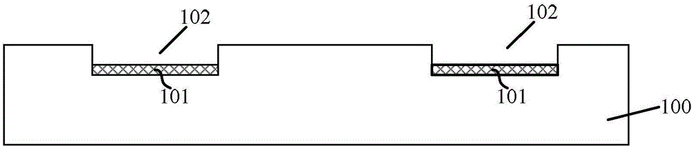
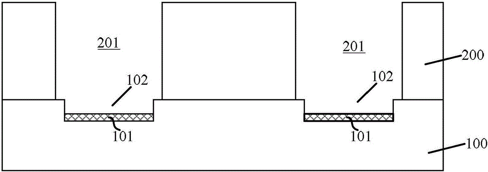
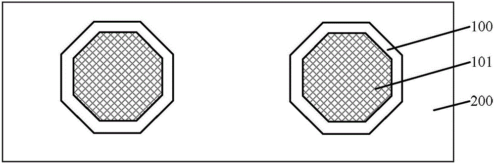
[0022] Please refer to figure 1 , A substrate 100 is provided, the surface of the substrate 100 has a groove 101, and the groove 102 exposes the surface of the metal layer 101.
[0023] The substrate 100 is a multilayer structure, including a semiconductor layer and a dielectric layer on the surface of the semiconductor layer, a semiconductor device in the semiconductor layer, a metal interconnect structure in the dielectric layer, and the like. The metal layer 101 is a bonding pad, which is used as a connection structure to an external circuit after packaging. The material of the metal layer 101 may be metals such as Al, Cu, or Au. The size of the metal layer 101 may be the same as the size of the groove 102 or may be larger than the size of the groove 102.
[0024] In another embodiment of the present invention, the base 100 includes a substrate and a passivation layer on the surface of the substrate, the substrate has a metal layer 101, and the groove 102 is located in the passivation layer to expose all The part of the surface of the metal layer. The material of the passivation layer may be silicon nitride or silicon oxide, etc., with a large thickness, which can play an effective stress buffering effect in subsequent packaging and other processes. By etching the passivation layer, a groove 102 is formed and the metal layer 101 is exposed.
[0025] The groove 102 exposes the surface of the metal layer 101, and the cross-sectional shape of the groove 102 is a regular polygon, such as a regular quadrilateral, a regular pentagon, a regular hexagon, a regular heptagon, a regular octagon, etc. The regular polygon is a symmetrical figure, and the stress distribution of the metal bumps subsequently formed in the groove 102 is relatively symmetric, which is easy to achieve a stress balance state. In this embodiment, the cross-sectional shape of the groove 102 is a regular octagon.
[0026] Please refer to figure 2 , Forming a mask layer 200 with an opening 201 on the surface of the substrate 100.
[0027] The material of the mask layer 200 may be photoresist, silicon oxide, silicon nitride, or the like. The method of forming the mask layer 200 includes: after forming a mask material layer on the surface of the substrate 100, etching the mask material layer to the surface of the substrate 100 to form an opening 201. The opening 201 exposes the groove 102 and a part of the base surface 100, the cross-sectional shape of the opening 201 is the same as the cross-sectional shape of the groove 102, and each side wall of the opening 201 is connected to the groove 102. The vertical distances between the side walls are equal.
[0028] The cross-sectional shape of the opening 201 is consistent with the cross-sectional shape of the groove 102, and may be a regular polygon, such as a regular quadrilateral, a regular pentagon, a regular hexagon, a regular heptagon, a regular octagon, and the like. In this specific embodiment, the cross-sectional shape of the opening 201 is a regular octagon.
[0029] Please refer to image 3 , Is a schematic top view after forming the mask layer 200.
[0030] The opening 201 (please refer to figure 2 ) And groove 102 (please refer to figure 2 The top view figure of) is two concentric regular octagons, and the edges are parallel to each other, so that the vertical distances between the side walls of the opening 201 and the side walls of the groove 102 are the same. Therefore, the stress distribution of the metal bumps subsequently formed in the opening 201 is uniform, which can alleviate the problem of fracture of the metal bumps.
[0031] If the vertical distance between the side wall of the opening 201 and the side wall of the groove 102 is too small, the contact area between the subsequently formed metal bumps and the surface of the substrate 100 is small, and the stress cannot be effectively relieved; and the side wall of the opening 201 The vertical distance between the sidewall of the groove 102 and the side wall is too large, or the subsequent formed metal bumps are large in volume, and the distance between adjacent metal bumps is too small, which may easily cause problems such as short circuits in the packaging process. In a specific embodiment of the present invention, the vertical distance between the side wall of the opening 201 and the side wall of the groove 102 may be 5 μm-10 μm, for example, 6 μm or 8 μm.
[0032] Please refer to Figure 4 , In the groove 102 (please refer to figure 2 ) And opening 201 (please refer to figure 2 In ), metal bumps 301 on the surface of the metal layer 101 and part of the surface of the substrate 100 are formed.
[0033] The metal bumps 301 are made of metal materials such as copper and gold, and the metal bumps 301 can be formed by an electroplating process. The cross-sectional shape of the metal bump 301 is the same as the cross-sectional shape of the opening 201 and is a regular polygon. Therefore, the vertical distance 101 between each side wall of the metal bump 301 and the side wall of the groove 102 is the same, that is, the distance between each side wall of the metal bump 301 and the edge of the metal layer 101 is the same, so that The stress distribution of the connecting interface between the metal bump 301 and the substrate 100 and the metal layer 101 is relatively uniform, so that the metal bump 301 is not prone to break or fall off.
[0034] Since the stress distribution between the metal bumps 301 and the substrate 100 is relatively uniform, there is no need to form an additional passivation layer on the surface of the substrate 100 to alleviate the effects of stress. Compared with the prior art, the process cost and production can be reduced. cycle.
[0035] In this embodiment, after the metal bump 301 is formed, a solder cap layer 302 is formed on the top of the metal bump 301, and the material of the solder cap layer 302 is tin or lead-tin alloy. After the solder cap layer material is formed on the surface of the metal bump 301 by an electroplating process, the solder cap layer material is heated to melt it into a hemispherical shape, and cooled and solidified, so that the solder cap layer 302 is a hemisphere shape.
[0036] Please refer to Figure 5 , The mask layer 200 is removed, and the surface of the substrate 100 is exposed.
[0037] The mask layer 200 is removed by an etching process. If the mask layer 200 is processed to be photoresist, the mask layer 200 can also be removed by an ashing process.
[0038] Please refer to Figure 6 to Figure 8 It is a schematic diagram of the formation process of a semiconductor structure according to another embodiment of the present invention.
[0039] Please refer to Image 6 In another embodiment of the present invention, before forming the mask layer 400, an under bump metal layer 500 covering the inner wall of the groove and the surface of the substrate 100 is formed.
[0040] The under-bump metal layer 500 may have a single-layer structure, such as a titanium layer, a titanium nitride layer, or a tungsten titanide layer. The under-bump metal layer 500 may also have a multi-layer structure. In this specific embodiment, the under-bump metal layer 500 includes a titanium layer or a copper layer on the surface of the titanium layer, and the sputtering process is used to form the Bump metal layer 500. The formation of the under-bump metal layer 500 can improve the conductivity of the bottom of the opening 201 on the one hand, and facilitate subsequent electroplating to form metal bumps; on the other hand, it can improve the adhesion between the subsequently formed metal bumps and the underlying material Sex.
[0041] Please refer to Figure 7 , In the opening 201 (please refer to Image 6 ) And groove 102 (please refer to Image 6 A metal bump 401 on the surface of the metal layer 500 under bump is formed inside.
[0042] The metal bumps 401 and the under-bump metal layer 500 have high adhesion, and problems such as falling off are unlikely to occur. In this embodiment, it further includes a solder cap layer 402 formed on the metal bump 401.
[0043] Please refer to Figure 8 , Remove the mask layer 400 (please refer to Figure 7 ), and a part of the under-bump metal layer 500 under the mask layer 400.
[0044] After the mask 400 is removed by a wet or dry etching process, the metal bump 401 is used as a mask to etch the under-bump metal layer 500, leaving some bumps under the metal bumps 401 Lower metal layer 501.
[0045] In the formation process of the above-mentioned semiconductor structure, a mask layer with openings is formed on the surface of the substrate, and the cross-sectional shape of the opening is the same as the cross-sectional shape of the groove, and each side wall of the opening is opposite to the side of the groove. The vertical distances between the walls are the same, so that the distances between the sidewalls of the metal bumps and the edges of the metal layer that are subsequently formed in the grooves and openings are the same, and the metal bumps are connected to the substrate and the metal layer at the same distance. The stress distribution is relatively uniform, so that the metal bumps are not prone to break or fall off.
[0046] The specific embodiment of the present invention also provides a semiconductor structure.
[0047] Please refer to Figure 5 , Is a schematic diagram of a semiconductor structure provided by an embodiment of the present invention.
[0048] The semiconductor structure includes: a substrate 100 with grooves on the surface of the substrate 100, and the grooves expose the surface of the metal layer 101; metal bumps 301 on the surface of the metal layer 101 and part of the surface of the substrate 100, the metal The cross-sectional shape of the bump 301 is the same as the cross-sectional shape of the groove, and the vertical distance between each side wall of the metal bump 301 and the side wall of the groove is equal.
[0049] The substrate 100 is a multilayer structure, including a semiconductor layer and a dielectric layer on the surface of the semiconductor layer, a semiconductor device in the semiconductor layer, a metal interconnect structure in the dielectric layer, and the like. The metal layer 101 is a bonding pad, which is used as a connection structure to an external circuit after packaging. The material of the metal layer 101 may be metals such as Al, Cu, or Au. The size of the metal layer 101 may be the same as the size of the groove, or may be larger than the size of the groove.
[0050] In another embodiment of the present invention, the base 100 includes a substrate and a passivation layer on the surface of the substrate, the substrate has a metal layer 101, and the groove is located in the passivation layer to expose the Part of the surface of the metal layer. The material of the passivation layer may be silicon nitride or silicon oxide, etc., with a large thickness, which can play an effective stress buffering effect in subsequent packaging and other processes. By etching the passivation layer, a groove is formed, exposing the metal layer 101.
[0051] The material of the metal bump 301 is a metal material such as copper and gold, and the cross-sectional shape of the metal bump 301 may be a regular polygon, such as a regular quadrilateral, a regular pentagon, a regular hexagon, a regular heptagon, and a regular octagon. 形等。 Shape and so on. In this specific embodiment, the cross-sectional shape of the metal bump 301 is a regular octagon.
[0052] The cross-sectional shape of the groove is the shape of the metal layer 101 exposed at the bottom of the groove, and the projections of the metal bump 301 and the exposed metal layer 101 on a plane parallel to the substrate 100 are two concentric The positive polymorphism of the metal bump 301 and the edges are parallel to each other, so that the vertical distances between the side walls of the metal bump 301 and the groove side wall are equal, that is, the side walls of the metal bump 301 and the metal layer 101 The distance between the edges of the metal bumps 301 is the same, so that the stress distribution of the connecting interface between the metal bumps 301 and the substrate 100 and the metal layer 101 is relatively uniform, so that the metal bumps 301 are not prone to break or fall off.
[0053] If the vertical distance between the side wall of the metal bump 301 and the side wall of the groove is too small, the contact area between the subsequently formed metal bump and the surface of the substrate 100 is small, and the stress cannot be effectively relieved; and the metal bump The vertical distance between the side wall of 301 and the side wall of the groove is too large or the volume of the subsequently formed metal bump is too large, and the distance between adjacent metal bumps is too small, which may easily cause problems such as short circuit in the packaging process. In a specific embodiment of the present invention, the vertical distance between the sidewall of the metal bump 301 and the sidewall of the groove may be 5 μm-10 μm, for example, 6 μm or 8 μm.
[0054] In this specific embodiment, the top of the metal bump 301 also has a solder cap layer 302, the solder cap layer 302 is hemispherical in shape, and the material is tin or lead-tin alloy.
[0055] Please refer to Figure 8 , Is a schematic diagram of a semiconductor structure in another specific embodiment of the present invention.
[0056] On the basis of the foregoing embodiment, the semiconductor structure further includes: an under bump metal layer 501 located between the metal bump 401 and the substrate 100. The top of the metal bump 401 has a solder cap layer 402.
[0057] The under-bump metal layer 501 may be a single-layer structure or a multi-layer structure. In this specific embodiment, the under-bump metal layer 501 includes a titanium layer or a copper layer on the surface of the titanium layer. The under-bump metal layer 501 can improve the conductivity between the metal bump 401 and the metal layer 101 on the one hand, and on the other hand, the under-bump metal layer 501 has higher adhesion to it, which can avoid metal bumps. The block 401 falls off.
[0058] The vertical distances between the sidewalls of the metal bumps of the above-mentioned semiconductor structure and the sidewalls of the grooves are the same, so that the distances between the sidewalls of the metal bumps and the edges of the bottom metal layer are the same. The stress distribution of the connection interface between the bump and the substrate and the metal layer is relatively uniform, so that the metal bump is not prone to breakage or fall off. In addition, the metal bumps and the substrate also include an under-bump metal layer, which can further improve the conductivity between the metal bumps and the metal layer, and the metal bumps and the under-bump metal layer have higher adhesion. Adhesion and metal bumps, thereby further improving the problem of easy fall-off of metal bumps.
[0059] The above are only the preferred embodiments of the present invention. It should be pointed out that for those of ordinary skill in the art, without departing from the principle of the present invention, several improvements and modifications can be made, and these improvements and modifications should also be considered This is the protection scope of the present invention.

PUM

no PUM

Description & Claims & Application Information

We can also present the details of the Description, Claims and Application information to help users get a comprehensive understanding of the technical details of the patent, such as background art, summary of invention, brief description of drawings, description of embodiments, and other original content. On the other hand, users can also determine the specific scope of protection of the technology through the list of claims; as well as understand the changes in the life cycle of the technology with the presentation of the patent timeline. Login to view more.

Similar technology patents

Ceramic fiber-coated suspension bridge main cable

PendingCN111021248AUniform distribution of temperature fieldUniform stress distribution
Owner:CHANGSHA UNIVERSITY OF SCIENCE AND TECHNOLOGY

Voice coil motor and leaf spring thereof

InactiveCN103051145AUniform stress distributionreduce stress concentration
Owner:SHENZHEN WEIMENG PHOTOELECTRIC TECH

Dual clutch having a load transfer plate immersing in sections and assembly formed by the dual clutch and a flywheel

ActiveCN109863325AIncreased radial structural space requirementsUniform stress distribution
Owner:SCHAEFFLER TECH AG & CO KG

Rolling type forklift side shifter

PendingCN112897405Areduce frictionUniform stress distribution
Owner:ANQING LIANDONG ENG TRUCKS ATTACHMENTS

Classification and recommendation of technical efficacy words

  • Uniform stress distribution

Connection device of prestress concrete and steel combination wind power generation tower

ActiveCN103994034AUniform stress distributionavoid uneven distribution
Owner:HUNAN UNIV

Biaxial drawing test piece for testing strength of thermal barrier coating

InactiveCN102928335AUniform stress distribution
Owner:XI AN JIAOTONG UNIV

Aqueous metal anticorrosive, rustproof and thermal insulation coating

InactiveCN110172285AUniform stress distributionreduce stress cracking
Owner:大余松瀛化工有限公司

Drill rod joint

InactiveCN102900379AUniform stress distributionstrong rigidity
Owner:TIANJIN DEHUA GASOLINEEUM EQUIP MFG
Why Eureka
Try Eureka