Thin film transistor

A technology of thin film transistors and semiconductors, applied in the direction of transistors, semiconductor devices, electric solid devices, etc., can solve the problems of not being able to improve the light transmittance of large-size TFTs, increase the area of ​​​​the GDM circuit frame, etc., to improve the curing rate of the frame glue and reduce the size , the effect of saving wasted space

Active Publication Date: 2016-12-21
NANJING CEC PANDA LCD TECH
View PDF4 Cites 15 Cited by
  • Summary
  • Abstract
  • Description
  • Claims
  • Application Information

AI Technical Summary

Problems solved by technology

However, the hollow area of ​​the capacitor increases the frame area occupied by the GDM circuit, which cannot improve the light transmittance of large-size TFTs.

Method used


Image

  • Thin film transistor
  • Thin film transistor
  • Thin film transistor

Examples


Embodiment 1

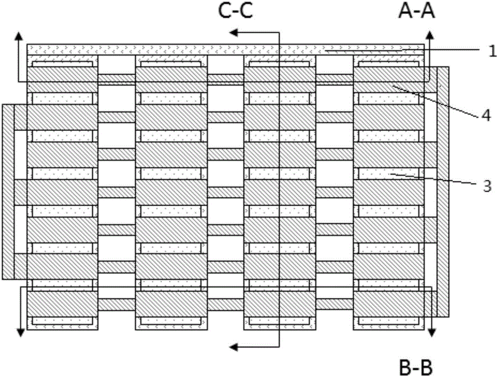
[0046] Such as Figure 1-4 As shown, it is a kind of thin film transistor of the present invention, which is a hollow type TFT with BCE structure, and there is no capacitance in the TFT. The hollow type TFT comprises a first metal layer gate (1), a first insulating layer gate insulating layer (2), a semiconductor layer (3), a second metal layer source drain (4) and a third insulating layer passivation layer (5); the first metal layer gate (1) is directly formed on the substrate glass layer (6), and the gate is formed from this layer of metal; the first insulating layer is located on the first metal layer gate (1) Above, a gate insulating layer is formed to separate the gate from the semiconductor layer (3); the semiconductor layer (3) is on the first insulating layer gate insulating layer (2); the second metal layer is used to form the source and drain , located on the semiconductor layer (3) directly in contact with the semiconductor layer (3), the third insulating layer pas...

Embodiment 2

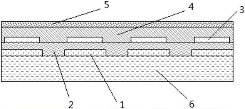
[0049] Such as Figure 5-8 As shown, an improved thin film transistor based on Example 1 is a hollowed-out TFT with a BCE structure, and there is a capacitor in the TFT. The difference between Example 2 and Example 1 is that the gate metal line and the source drain The pole metal lines overlap, and the overlap forms a capacitor. Between the TFTs, a capacitor is formed due to the overlapping of the gate metal line and the source-drain metal line, and the capacitor is jointly formed by the first metal layer, the first insulating layer and the second metal layer. Because part of the capacitance has been formed in the TFT, the size of the original capacitance of the GDM circuit can be reduced in this way, thereby further reducing the frame width.

Embodiment 3

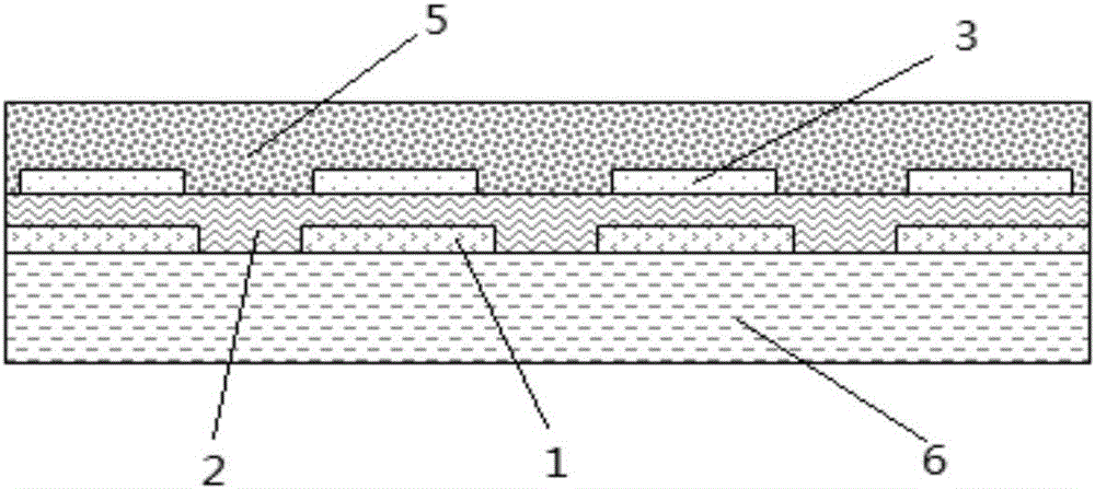
[0051] Such as Figure 9-12 As shown, it is a thin film transistor of the present invention, which is a hollow TFT with ES structure, and there is no capacitor in the TFT. The hollow-out TFT comprises a first metal layer gate (1), a first insulating layer gate insulating layer (2), a semiconductor layer (3), a second insulating layer etch barrier layer (7), and a second metal layer source The drain (4) and the third insulating layer passivation layer (5), the first metal layer gate (1) is directly formed on the substrate glass layer (6), and the gate is formed by this layer of metal; the first The insulating layer is located on the gate (1) of the first metal layer to form a gate insulating layer to separate the gate from the semiconductor layer; the semiconductor layer (3) is on the first insulating layer gate insulating layer (2); the second metal layer , for forming source and drain electrodes, located on the second insulating layer etching barrier layer (7), through the e...


PUM


Abstract

The invention discloses a thin film transistor (TFT), which comprises a first metal layer gate, a first insulation layer gate insulation layer, a semiconductor layer, a second metal layer source and drain and a third insulation layer passivation layer, wherein the first metal layer gate is formed on a substrate glass layer; the first insulation layer gate insulation layer is located on the first metal layer gate; the semiconductor layer is on the first insulation layer gate insulation layer; the second metal layer source and drain is located on the semiconductor layer; the third insulation layer passivation layer is in the outermost layer to be located on the second metal layer source and drain; and the first metal layer gate and the semiconductor layer are set to have hollow structures. The thin film transistor designs the gate and the semiconductor layer in hollow forms, multiple distributively-arranged light through holes are formed inside the TFT, the transmittance of ultraviolet light used by sealant curing can be enhanced, and the curing rate of the sealant applied to the TFT is improved. The hollow TFT can enable the sealant applying area to be thoroughly overlapped with the TFT, and the frame width can be further reduced.

Description

technical field [0001] The invention relates to a flat panel display, in particular to a thin film transistor. Background technique [0002] At present, small and medium-sized display panels have higher and higher requirements for narrow bezels. In order to reduce the frame size, the GDM (Gate Driver Monolithic) circuit is used on the panel instead of the IC chip as the driving circuit of the scanning line. The GDM circuit is composed of a thin film transistor (TFT, Thin Film Transistor) and a capacitor, and is directly built on the gate drive circuit on the frame of the TFT substrate AA (ActiveArea, LCD display area), which occupies a smaller frame size than the IC. The GDM circuit reduces the width of the panel frame to a certain extent. [0003] However, because the GDM circuit contains several large-area TFTs and capacitors, it will reduce the transmittance of ultraviolet light during the curing process of the sealant, and the coating area of ​​the sealant cannot overl...

Claims


Application Information

Patent Timeline
Patent Type & Authority Applications(China)
IPC IPC(8): H01L29/786H01L29/06H01L29/423
CPCH01L29/0684H01L29/42384H01L29/786H01L27/1222H01L27/1248G02F2201/086G02F2201/124G02F1/1368H01L27/1225H01L27/1255H01L29/41733H01L29/7869H01L29/78696G02F1/13454G09G2310/0267G09G2310/0281G09G2310/0283G09G2310/0286G09G3/3677
Inventor 黄洪涛戴超
Owner NANJING CEC PANDA LCD TECH
Why Eureka
Try Eureka