Manufacturing method and system of large-area perovskite solar cell
A technology of a solar cell and a manufacturing method, applied in the field of solar cells, can solve problems such as lack of industrialization potential, and achieve the effect of improving large-area uniformity and preparation rate
- Summary
- Abstract
- Description
- Claims
- Application Information
AI Technical Summary
Problems solved by technology
Method used
Image
Examples
Embodiment 1
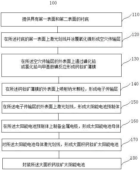
[0045] 1. FTO (30*60cm) glass is scribed P1 by laser (1024 red light), the line spacing is 1cm, and then the hole transport layer is prepared by magnetron sputtering in the hole transport layer preparation chamber 4. The material of the hole transport layer is nickel oxide, and the preparation method is sputtering, scraping or spraying, or inkjet printing, and the thickness of the prepared nickel oxide is 70-80nm.
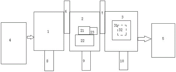
[0046] 2. After that, the sample enters the sampling chamber 1, and the sampling chamber 1 and the first evaporation chamber 2 are simultaneously evacuated to 1E-7torr, and the first transfer door 6 between the sampling chamber 1 and the first evaporation chamber 2 is opened. The sample enters the first evaporation chamber 2, the first transfer door 6 is closed, and the baffle (not shown) on the substrate is closed.
[0047] 3. Put lead iodide or lead chloride powder in the sublimation tank 22, vacuumize, heat to 310 degrees, wait for the lead iodide or lead chlori...
PUM
| Property | Measurement | Unit |
|---|---|---|
| Thickness | aaaaa | aaaaa |
| Diameter | aaaaa | aaaaa |
Abstract
Description
Claims
Application Information

