Transparent broadband metamaterial absorber

A technology of transparent conductive materials and metamaterials, applied in electrical components, antennas, etc., can solve problems such as manufacturing difficulties, deterioration of light transmission performance, and high cost of transparent absorbers, and achieve convenient processing, excellent light transmission performance, and excellent environmental adaptability sexual effect

Inactive Publication Date: 2016-12-21
JIANGSU SAIBO DEFENSE TECH CO LTD
View PDF1 Cites 32 Cited by
  • Summary
  • Abstract
  • Description
  • Claims
  • Application Information

AI Technical Summary

Problems solved by technology

[0002] Most of the traditional multi-resonant structures use multi-layer stacking technology to achieve bandwidth expansion, which is expensive for transparent absorbers, difficult to manufacture, and seriously degraded in light transmission performance.

Method used


Image

  • Transparent broadband metamaterial absorber
  • Transparent broadband metamaterial absorber
  • Transparent broadband metamaterial absorber

Examples


Embodiment 1

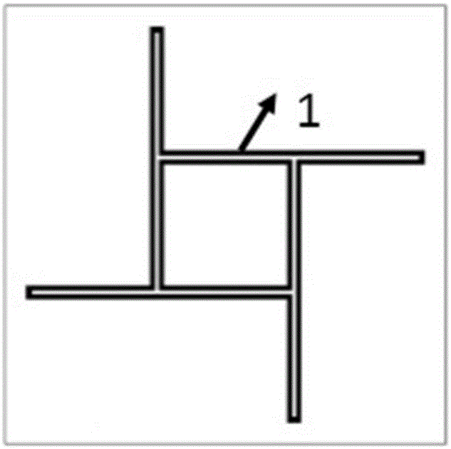
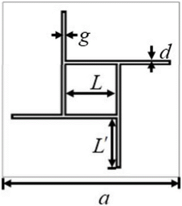
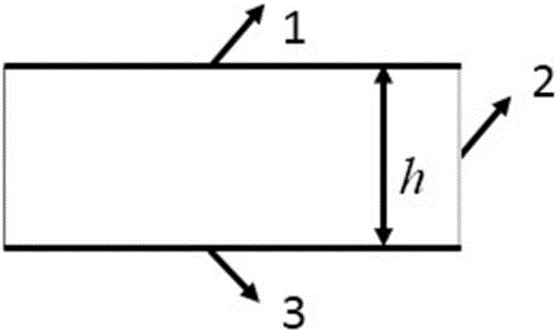
[0021] Embodiment 1: The transparent broadband metamaterial absorber is a single-layer transparent broadband metamaterial absorber, including a plurality of periodically arranged cell structures, such as Figure 4 shown. The unit structure includes an upper transparent resonant structure 1 located in the center of the unit structure, a middle transparent substrate 2 and a lower transparent reflective layer 3, the upper transparent resonant structure 1 is located above the middle transparent substrate 2, and the lower transparent reflective layer 3 is located Below the middle transparent substrate 2, such as Figure 1b As shown; the upper transparent resonant structure 1 is a symmetrical figure, including a ring and a ring with branches on the periphery of the ring. The upper transparent resonant structure 1 in this embodiment is a square ring and a square ring with branches located on the periphery of the square ring. Such as Figure 1a The shape of the windmill can also be o...

Embodiment 2

[0024] Embodiment 2: The transparent broadband metamaterial absorber is a three-layer transparent broadband metamaterial absorber, including a plurality of periodically arranged unit structures, such as Figure 6 shown. The unit structure includes an upper transparent resonant structure 4 located at the center of the unit structure, an upper transparent substrate 5, a middle transparent substrate 6, a lower transparent substrate 7 and a lower transparent reflective layer 8, and the upper transparent resonant structure 4 is located between the upper transparent substrate 5 and the lower transparent reflective layer 8. Between the middle transparent substrate 6, the lower transparent reflective layer 8 is located between the middle transparent substrate 6 and the lower transparent substrate 7, such as Figure 2b As shown; the upper transparent resonant structure 4 is a symmetrical figure, including a ring and a ring with branches on the periphery of the ring. The upper transpare...


PUM


Abstract

The invention discloses a transparent broadband metamaterial absorber which comprises multiple periodically arranged unit structures. Each of the unit structures comprises an upper layer transparent resonant structure at the center of the unit structure, a middle layer transparent substrate, and a lower layer transparent reflection layer. The upper layer transparent resonant structure is above the middle transparent substrate, and the lower layer transparent reflection layer is under the middle layer transparent substrate. The upper layer transparent resonant structure is a symmetric figure which comprises a ring and a ring with a branch at the periphery of the ring. Both the upper layer transparent resonant structure and the lower layer transparent reflection layer are transparent conductive materials. According to the transparent broadband metamaterial absorber, the reflection rate of incident electromagnetic wave can be effectively attenuated in an X band, the transparent broadband metamaterial absorber is convenient to manufacture, the technology is mature, the light transmittance performance of the overall structure is excellent and a light transmittance rate is larger than or equal to 80% in a visible light range, and the transparent broadband metamaterial absorber has a good prospect in application.

Description

technical field [0001] This patent relates to radar stealth and new artificial electromagnetic materials, in particular to a transparent broadband material absorber. Background technique [0002] Most of the traditional multi-resonant structures use multi-layer stacking technology to achieve bandwidth expansion, which is expensive for transparent absorbers, difficult to manufacture, and will seriously deteriorate the light transmission performance. [0003] The new artificial electromagnetic materials (Metamaterials) involved in the present invention are composed of periodic arrangement of sub-wavelength unit structures of a certain scale. By manually designing the unit structure, the equivalent dielectric constant, magnetic permeability, refractive index and wave impedance of the material can be controlled. And other electromagnetic parameters, realize the properties that the materials that exist in nature do not have. With the deepening of theoretical research and applica...

Claims


Application Information

Patent Timeline
Patent Type & Authority Applications(China)
IPC IPC(8): H01Q17/00
CPCH01Q17/00
Inventor 程强张琤杨萍亓培培崔铁军周小阳
Owner JIANGSU SAIBO DEFENSE TECH CO LTD
Why Eureka
Try Eureka