
Embedded PIP capacitor CMOS manufacturing method

A manufacturing method and capacitor technology, applied in the direction of capacitors, circuits, electrical components, etc., can solve the problems of distribution influence, influence device performance, differences, etc., and achieve the effect of reducing differences and improving performance

Active Publication Date: 2016-12-28
FOUNDER MICROELECTRONICS INT
View PDF4 Cites 0 Cited by
  • Summary
  • Abstract
  • Description
  • Claims
  • Application Information

AI Technical Summary

Problems solved by technology

[0010] The disadvantage of the traditional PIP-embedded CMOS manufacturing process is that during the thermal process of growing the dielectric layer and depositing the second layer of polysilicon, the distribution of the implanted threshold ions will be affected, resulting in the CMOS device parameters and standard embedded PIP capacitance There are differences between CMOS device parameters without PIP capacitors, which affect device performance

Method used


Image

  • Embedded PIP capacitor CMOS manufacturing method
  • Embedded PIP capacitor CMOS manufacturing method
  • Embedded PIP capacitor CMOS manufacturing method

Examples


Embodiment Construction

[0036] In order to make the purpose, technical solutions and advantages of the embodiments of the present invention clearer, the technical solutions in the embodiments of the present invention will be clearly and completely described below in conjunction with the drawings in the embodiments of the present invention. Obviously, the described embodiments It is a part of embodiments of the present invention, but not all embodiments. Based on the embodiments of the present invention, all other embodiments obtained by persons of ordinary skill in the art without making creative efforts belong to the protection scope of the present invention.

[0037] Those skilled in the art should understand that: the following examples are specific descriptions of the core technical solutions of the present invention, and those involving existing specific manufacturing processes will not be described in detail.

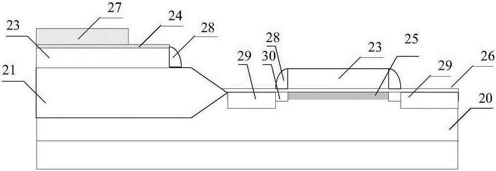
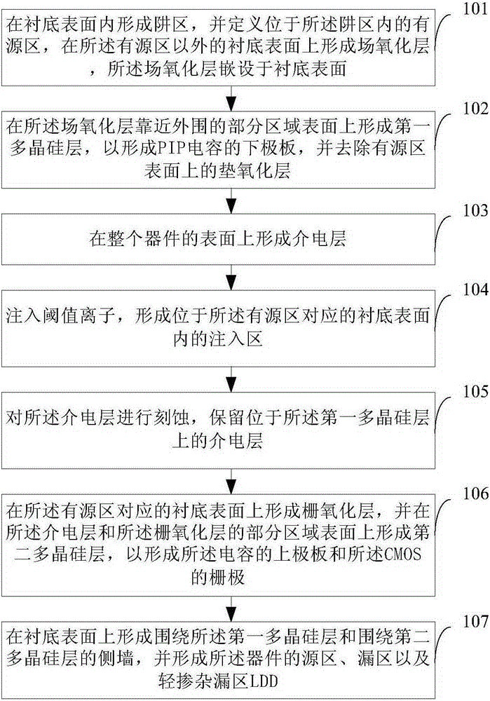
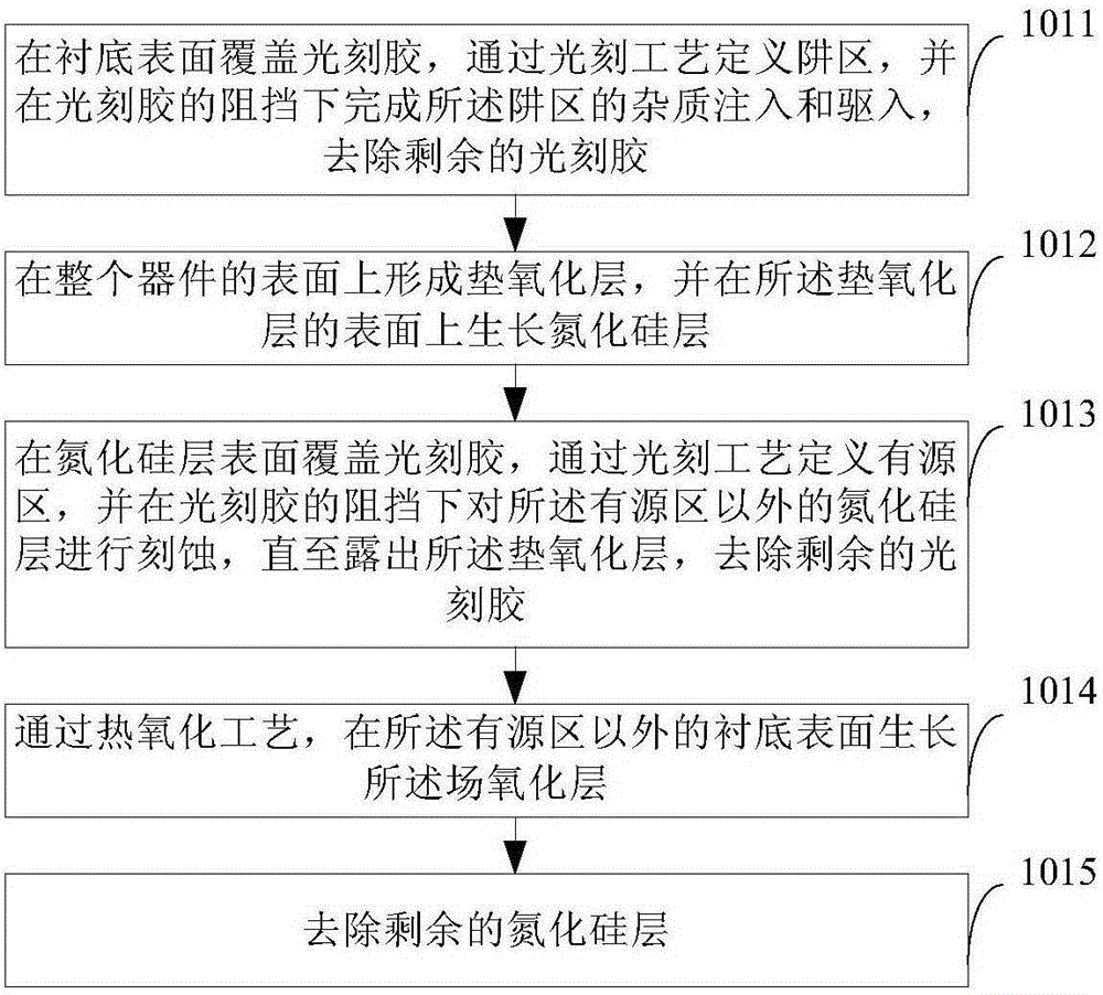
[0038] figure 2 A schematic flow chart of a CMOS manufacturing method for embeddin...


PUM


Abstract

The invention provides an embedded PIP capacitor CMOS manufacturing method. The method comprises the steps that a well region is formed in the surface of a substrate and an active region in the well region is defined, and a field oxide layer is formed on the surface of the substrate apart from the active region; a first polysilicon layer is formed on the surface of the partial region of the field oxide layer close to the periphery, and a mat oxide layer on the surface of the active region is removed; a dielectric layer is formed on the surface of the whole device; threshold ions are injected so that an injection region in the surface of the substrate corresponding to the active region is formed; the dielectric layer is etched and the dielectric layer on the first polysilicon layer is reserved; a gate oxide layer is formed on the surface of the substrate corresponding to the active region, and a second polysilicon layer is formed on the surface of the partial region of the dielectric layer and the gate oxide layer; and side walls enclosing the first polysilicon layer and enclosing the second polysilicon layer are formed on the surface of the substrate, and a source region, a drain region and a lightly doped drain region LDD of the device are formed. The influence of the conventional technology on the threshold ion distribution can be avoided and the performance of the device can be enhanced.

Description

technical field [0001] The invention relates to the field of semiconductor manufacturing, in particular to a CMOS manufacturing method for embedding PIP capacitors. Background technique [0002] Polysilicon-dielectric layer-polysilicon (Polysilicon-Insulator-Polysilicon, referred to as PIP) capacitor is a structure, with a layer of polysilicon as the lower plate, another layer of polysilicon as the upper plate, and a thinner oxide layer in the middle is the capacitance of the dielectric layer. In the existing technology, PIP capacitors are usually embedded in complementary metal oxide semiconductor devices (Complementary Metal Oxide Semiconductor, referred to as CMOS), which are used for frequency modulation and to prevent noise emission from analog circuits. [0003] In the CMOS manufacturing process of embedded PIP, the traditional method is to grow an oxide layer as the dielectric layer of the PIP capacitor after etching the gate polysilicon, and then deposit a layer of ...

Claims


Application Information

Patent Timeline
IPC IPC(8): H01L21/8238H01L21/02
CPCH01L21/8238H01L28/40
Inventor 马万里闻正锋赵文魁
Owner FOUNDER MICROELECTRONICS INT
Features
  • Generate Ideas
  • Intellectual Property
  • Life Sciences
  • Materials
  • Tech Scout
  • Unparalleled Data Quality
  • Higher Quality Content
  • 60% Fewer Hallucinations
Learn More