Contact-probe type temperature detector, semiconductor device evaluation apparatus and semiconductor device evaluating method

A technology of temperature detector and evaluation device, which is applied in the direction of measuring device, thermometer parts, and single semiconductor device testing, etc., can solve problems such as inability to set, difficult to suppress gas discharge, and inability to detect temperature of semiconductor components, and achieve high precision The effect of detection

Inactive Publication Date: 2017-01-04
MITSUBISHI ELECTRIC CORP
View PDF11 Cites 6 Cited by
  • Summary
  • Abstract
  • Description
  • Claims
  • Application Information

AI Technical Summary

Problems solved by technology

Therefore, the temperature of the semiconductor element itself cannot be detected with high precision.
[0013] In addition, the measurement systems based on the cantilever method described in Patent Document 3 to Patent Document 5 need to tilt the probe according to the principle of the cantilever method, and when measuring the electrical characteristics of a high-voltage device, there is a problem that , since the distance between the inclined portion of the probe and the object to be measured cannot be set arbitrarily, it is difficult to suppress gas discharge

Method used


Image

  • Contact-probe type temperature detector, semiconductor device evaluation apparatus and semiconductor device evaluating method
  • Contact-probe type temperature detector, semiconductor device evaluation apparatus and semiconductor device evaluating method
  • Contact-probe type temperature detector, semiconductor device evaluation apparatus and semiconductor device evaluating method

Examples


Embodiment Construction

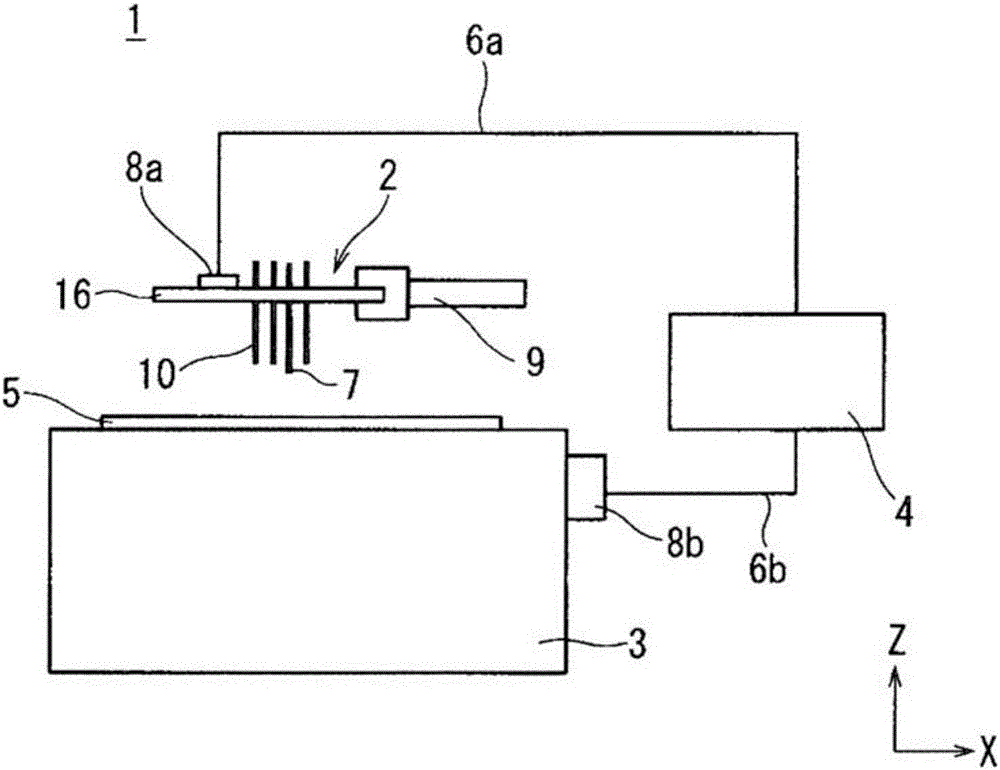
[0037] Hereinafter, embodiments of the present invention will be described using the drawings. figure 1 It is a schematic diagram of the evaluation device 1 of the semiconductor device according to the embodiment.

[0038] In this embodiment, an example is shown in which a spring-type temperature detection probe 7 is arranged on the insulating plate 16, and the temperature of the semiconductor device 5 is measured before and during the evaluation of the electrical characteristics of the semiconductor device 5 as the object to be measured. The temperature of the surface is detected. In addition, in the present embodiment, the semiconductor device 5 with a vertical structure in which a large current flows in the longitudinal direction of the semiconductor device 5, that is, in the out-of-plane direction is shown as an example, but it is not limited thereto. A semiconductor device with a horizontal structure in which input and output are carried out on one side.

[0039] The ev...


PUM


Abstract

The invention provides techniques capable of suppressing aerial discharge in evaluating electric characteristics of semiconductor devices and capable of detecting the temperatures of semiconductor devices with higher accuracy. A temperature detecting probe (7) as a contact-probe type temperature detector includes a plunger portion (12) contactable with a semiconductor device (5) as an object to be measured, a spring member (17) placed on a base end portion of the plunger portion (12), a barrel portion (14) pressing the plunger portion (12) the semiconductor device (5) side with the spring member (17) interposed therebetween, and a thermocouple (19) as a temperature measuring portion detecting a temperature of the semiconductor device (5).

Description

technical field [0001] The present invention relates to a technique for detecting the temperature of a semiconductor device when evaluating the electrical characteristics of the semiconductor device. Background technique [0002] When evaluating the electrical characteristics of a semiconductor device as an object to be measured, it is important to detect the temperature of the semiconductor device with high accuracy. In particular, in the evaluation of the temperature characteristics, if the temperature detection during the evaluation is unstable, the temperature characteristics themselves contain errors. In addition, when evaluating electrical characteristics, the temperature of the semiconductor device may change due to the application of a large current and high voltage. In this case, it is also important to detect the temperature change of the semiconductor device together with the electrical characteristics. [0003] Under the above circumstances, as a method of dete...

Claims


Application Information

Patent Timeline
Patent Type & Authority Applications(China)
IPC IPC(8): G01R31/26G01K7/22G01K7/18
CPCG01K1/143G01K7/02H01C7/008G01R31/2601G01K7/18G01K7/22
Inventor 山下钦也野口贵也冈田章秋山肇上野和起
Owner MITSUBISHI ELECTRIC CORP
Why Eureka
Try Eureka